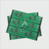
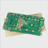
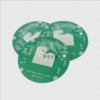
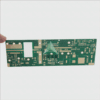
PCB stencil is an important tool used to make PCB circuit boards. So today, PEAK will introduce to you what is PCB stencil, as well as explain his advantages and uses.
A PCB stencil is a mesh structure made of woven metal or alloy wires that usually matches the printed pattern of the PCB. The stencil is placed on the printed circuit board to guide and position the solder paste to ensure that components adhere properly to the PCB surface. The opening and arrangement of the stencil determines the distribution of solder paste on the PCB, which is directly related to solder quality and assembly accuracy. By controlling the stencil’s parameters such as thickness, aperture and line width, different sizes and shapes of solder paste printing can be realized to meet various PCB design requirements.
Stencils for PCBs have the following advantages and multiple uses:
Advantages:
- precise positioning: the stencil has an accurate aperture and opening layout, which can ensure that the solder paste is printed in the correct position, thus realizing the precise positioning of components.
- uniform distribution: by controlling the aperture and line width of the stencil, you can realize the uniform distribution of solder paste, improve the quality and reliability of welding.
- efficient production: stencil can quickly and accurately print a large number of PCB, improve manufacturing efficiency and production speed.
- Consistency and Repeatability: the stencil design and manufacturing process is precisely controlled to ensure that the printing results of each PCB are consistent and repeatable.
Uses:
1. Solder Paste Printing: Stencils are used to print solder paste on the surface of PCBs to provide soldering points for SMT (Surface Mount Technology) assembly.
2. Component Positioning: The aperture and layout of the stencil corresponds to the location of the components on the PCB and is used to accurately position and align the components.
3. Solder Resist Printing: In addition to solder paste printing, stencils can be used to print solder resists to protect and isolate specific areas on a circuit board.
4. Inspection and quality control: The printed pattern on the stencil can be used to inspect and verify the quality of the PCB to ensure that the solder paste is distributed correctly and meets the requirements.
PCB stencil in the PCB manufacturing process plays a key role in positioning, printing and quality control, improve production efficiency and consistency, and to ensure the quality of welding and assembly precision.

