The Complete Guide to Etching PCB – A Step-by-Step Process for DIY Enthusiasts
PCB etching is an indispensable skill for creating custom printed circuit boards (PCBs) at home, giving DIY enthusiasts the power to design and fabricate PCBs without outsourcing fabrication services. In this guide, we’ll walk through each step of PCB etching from creating the layout to etching copper traces – whether you’re hobbyist or maker this guide will arm you with everything needed to design and manufacture your own PCBs!
1. Etching PCB: Design of PCB Layout
The initial step in PCB etching involves designing its layout with dedicated software such as EAGLE, KiCad or Altium Designer. Throughout this process it’s important to consider factors such as:
- Schematic Design: Draft a schematic diagram of your circuit, detailing all its components and their connections.
- PCB Layout: Convert the schematic into a PCB layout by arranging and routing components and connections as described by their diagram, taking care to ensure proper spacing, orientation and clearance between components.
- Copper Traces: Conceive copper traces that will transport electrical signals between components and optimize their width and spacing based on current requirements.
- Component Footprints: Choose appropriate component footprints or create custom footprints as necessary, with accurate pad sizes and orientations for soldering.
2. Etching PCB: Printing Your PCB Design
Once your layout has been approved, the next step in printing it should be printing onto transfer paper or transparency sheet using these steps:
- Prepare Printing Media: Select either specialized transfer paper or transparency sheet suitable for transferring PCB designs onto copper-clad boards.
- Print the Design: For optimal results, print the PCB design onto transfer paper using either a laser printer or an inkjet printer with waterproof ink and ensure it appears in reverse (mirror-imaged).
- Cut the Printed Design Accurately: When cutting the printed design to fit perfectly onto a copper-clad board, be precise with its size.
3. Etching PCB: Copying Your Design onto the Copper-Clad Board
Coupling PCB designs onto copper-clad boards is a key component of the etching process. Here’s how you do it:
- Clean the Copper-Clad Board: Before assembly, ensure that the copper surface of your board is free from dirt or oxidation by using fine sandpaper or PCB cleaning solutions to achieve maximum results.
- Apply Heat and Pressure: Place the printed design (ink side down) onto the copper surface of the board and use an iron or laminator to heat transfer ink onto copper by pressing down firmly with an iron or laminator. Pressing too lightly could result in ink being transferred by accident!
- Cooling and Peeling: After the board has cooled down, gently peel off the transfer paper until only your design remains attached to the copper surface.
4. Etching PCB: Etching Copper Traces
Succinctly put, etching copper traces is the process of extracting unnecessary copper from an electronic board while leaving behind only those desired traces. Follow these steps:
- Create an Etchant Solution: Combine an appropriate etchant solution such as ferric chloride or ammonium persulfate according to manufacturer’s directions, wearing gloves and goggles while handling these chemicals.
- Etching Process: Submerge your copper-clad board in an etchant solution and gently stir to facilitate its etching process. Monitor its progress periodically by inspecting its board carefully.
- Etching Completion: Once all unwanted copper has been completely etched away from the board, remove it from the etchant solution and rinse thoroughly with water to complete the etching process.
5. Etching PCB: Cleaning and Inspection
Once an etched PCB has been assembled, additional steps should be taken for its cleaning and inspection before processing further. Please follow these instructions:
- Removing Ink Residue: Use an appropriate ink remover or acetone to safely clean off ink residue from copper surfaces, taking care not to damage or disturb etched traces in any way.
- Visual Inspection: Conduct a visual inspection to ensure the etched traces are well-defined, free from short circuits, excessive etching or any short-circuits; any defects should be rectified as necessary.
6. Etching PCB: Drilling and Finishing
The final steps involve drilling holes for component mounting and adding finishing touches to the PCB. Here are the steps:
- Drill Holes: To effectively drill holes for component leads, utilize an appropriate PCB drill bit with appropriate drill bit size and ensure accurate placement and appropriate hole sizes.
- Silkscreen or Mask Application: Silkscreening or solder mask applications may help add labels and improve soldering accuracy.
- Final Inspection: Before finalizing and soldering components to the PCB, conduct a final visual inspection to make sure it’s suitable for assembly.
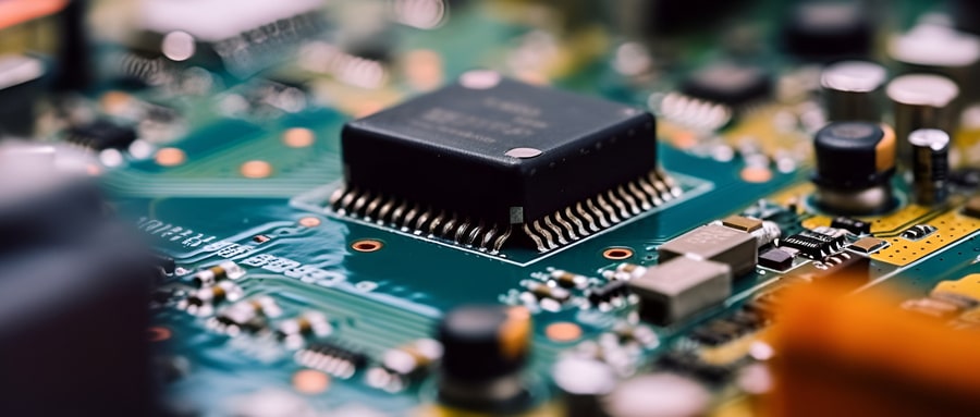
PCB etching is an exciting and fulfilling DIY hobby that allows DIY enthusiasts to design custom printed circuit boards from scratch. By following the step-by-step procedure outlined here, you can successfully etch your own PCBs from the ground up! Be patient as attention to detail is the key to producing high-quality results; practice will unlock creativity while building unique electronic projects with confidence.
Etching PCB FAQ:
- What is etching PCB manufacturing?
Etching PCB is the process of removing unwanted copper from a printed circuit board (PCB) to leave behind the desired circuit pattern. It is a crucial part of the PCB fabrication process and ensures precise circuit paths. - What chemicals are commonly used for etching PCBs?
The most commonly used chemicals for etching PCBs are ferric chloride (FeCl3), ammonium persulphate, or solutions of hydrochloric acid and hydrogen peroxide. - How does the etching PCB process work in PCB manufacturing?
The PCB is coated with a light-sensitive resist material, and then exposed to light through a mask that shows the circuit pattern. The exposed areas harden and become resistant to the etching solution. The board is then immersed in the etching chemical, which dissolves the unprotected copper, leaving the desired copper pattern. - Is it safe to etch PCBs at home?
While it is possible to etch PCBs at home using readily available chemicals, it isn’t generally recommended due to the safety risks involved. The chemicals used for etching are corrosive and must be handled with appropriate safety equipment and disposal practices. - Can the etching process affect the performance of a PCB?
Yes. Over or under etching can result in the copper traces being too thin, too wide, or even broken, which can affect the PCB’s performance or make it entirely non-functional. - How is the etching solution disposed of after use?
Etching solutions contain dissolved copper, which is hazardous. Therefore, they should never be poured down the drain. Disposal should be done following local hazardous waste regulations. - What is the role of the etching process in PCB multilayer stackup?
In a multilayer PCB, each layer of the copper foil is independently etched to create the specific circuit pattern for that layer. The layers are then laminated together to form the complete stackup. - Are there methods other than chemical etching for creating PCBs?
Yes, newer methods like laser etching and mechanical milling are alternatives to chemical etching. They physically remove unwanted copper rather than dissolving it, and they offer higher precision and avoid the use of hazardous chemicals. - How important is it to monitor the etching process?
It’s crucial, as the etching rate can change over time based on factors like the composition of the etching solution and its temperature. Regular monitoring ensures the etching process stays within its desired parameters. - What happens after etching in the PCB manufacturing process?
After etching, the remaining photoresist is stripped off, leaving the bare copper circuit. The board then undergoes a series of finishing tasks such as solder mask application, silkscreen printing, and final testing, leading to a finished functioning PCB.

