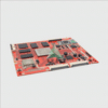
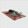
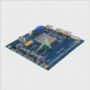
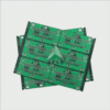
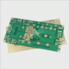
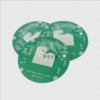
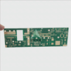
BGA PCBs (Ball Grid Array Printed Circuit Boards) have become an integral component of modern electronic devices, revolutionizing how components are mounted onto circuit boards while making devices more compact, efficient, and reliable. In this article, we’ll delve into the fundamentals of BGA PCBs; their structure, applications and key considerations.
1. What is a BGA PCB?
- BGA PCB packaging is an advanced integrated circuit packaging method that relies on solder balls arranged in an array, creating a higher density of connections than traditional methods.
- BGA PCBs are distinguished by their compact size, high performance, and advanced thermal management capabilities. They are widely utilized for applications including consumer electronics, automotive systems, telecommunications, aerospace systems and many others.
2. Benefits of BGA PCB Technology
- Increased Component Density: BGA PCBs enable higher component densities on smaller boards, enabling complex designs.
- Improved Electrical Performance: BGA packages feature shorter signal paths, which decrease the risk of signal degradation while improving overall electrical performance.
- Improved Thermal Management: Solder balls on a BGA PCB act as thermal vias, effectively dissipating heat and preventing overheating of the integrated circuits (ICs).
- Improved Reliability: Solder balls provide more secure and robust connections, decreasing risk from vibration, mechanical stress and temperature variations.
3. Key Considerations in BGA PCB Design
- PCB Layout: Trace placement and routing are of critical importance in BGA PCB designs, taking into account factors like signal integrity, thermal management and power distribution.
- Soldering Process: BGA packages require precise soldering techniques in order to maintain proper alignment and reliable connections. Reflow soldering and X-ray inspection are two such processes often used.
- Inspection and Rework: Due to the hidden nature of BGA packages, inspection and rework can be challenging. For this purpose, X-ray machines and other specialized equipment are used for thorough examination and, if needed, repairs.
4. Trends and Future Strategies in BGA PCB Technology
- Miniaturization: With electronic devices becoming smaller and more powerful, BGA PCBs will play a vital role in making them possible.
- Advanced Materials: By employing innovative materials like high-temperature solder alloys and flexible substrates, BGA PCBs’ performance and reliability will be further increased.
- Package-on-Package (PoP) Technology: PoP combines multiple BGA PCBs vertically, increasing connectivity and functionality without increasing footprint size.

BGA PCB technology has revolutionized the electronics industry, creating smaller, more powerful, and reliable devices. Engineers can harness its potential by understanding basic principles of BGA PCBs and considering key design factors; by doing this, cutting-edge electronic products will emerge! Embark upon an exciting journey of innovation and efficiency!
FAQ:
- What is a BGA in PCB manufacturing?
BGA stands for Ball Grid Array. It’s a type of surface mount packaging for integrated circuits that allows for more interconnection pins than older packaging types. The bottom side of the BGA package has a multitude of solder balls that attach to corresponding lands on the PCB. - Why are BGAs used?
BGAs are used as they offer a higher density of pins than older packages. Because of their grid layout, they can contain more interconnects in a smaller space, making them ideal for intricate, high-speed circuitry. These packages also exhibit better thermal and electrical performance. - What are the challenges in BGA PCB design?
BGA packages can be difficult to work with due to their higher complexity and fine pitch. Ensuring proper alignment between the BGA and the PCB is crucial. Moreover, soldering and de-soldering BGAs can be challenging due to hidden solder joints, which can also make inspection difficult. - What is BGA rework?
BGA rework is the process of removing a BGA from a PCB and replacing it with a new one. This can be a complex process due to the hidden solder joints, requiring specialized equipment like a rework station and X-ray machine for inspecting the soldering quality. - What is BGA soldering?
BGA soldering is the process of attaching a BGA package to a PCB using heat to melt the solder balls on the BGA package and the corresponding lands on the PCB. This requires precise control of the heat profile to ensure proper melting and adhesion. - What is the process of BGA Assembly?
BGA assembly involves applying solder paste to the PCB, accurately placing the BGA onto the solder, and then using a reflow oven to heat the assembly and melt the solder, causing it to adhere to the joint. - What is X-Ray Inspection in BGAs?
X-Ray inspection is used in BGA assembly to inspect the solder joints, which are hidden under the BGA package. It allows for profiling of the solder joints and detection of solder defects like opens or shorts, voids within the solder, and insufficient or excess solder. - What type of PCBs can BGAs be used on?
BGAs can be used on any type of PCB (rigid, flexible, or rigid-flex) that can handle the mechanical, thermal, and electrical requirements of the BGA package. - What are some common problems in BGA Assembly?
Common problems in BGA Assembly could include bridging (solder shorts), voids in solder balls, and poor joint strength. Misalignment of the BGA on the PCB can also occur due to movement during reflow. - What are Micro BGAs?
Micro BGAs are a very small type of BGA package with a significantly smaller footprint and lower profile than standard BGAs. These are used in highly space-constrained applications like laptops, smartphones, and other wearable devices.

