Solder Mask PCB: A Deep Dive into Its Impact on PCB Manufacturing Efficiency and Reliability
1. Solder Mask as the Unsung Hero of PCB Production
Definition of Solder Mask: Solder masks serve a vital purpose during PCB manufacturing by protecting critical copper traces against unsolicited solder bridge formation and potential circuit shorts. They do this through various protective layers that work in concert – resists, stops and multi-layered protective layers all help.
The Value Proposition: Solder mask’s value extends beyond soldering processes to provide essential protection from factors like dust, moisture and accidental handling that might threaten its lifespan or mechanical reliability of PCBs.
2. Various Aspects of Solder Mask PCB
Liquid Photoimageable (LPI) Solder Masks are well-renowned for their superior resolution, pinhole resistance, and high throughput performance, making them an invaluable asset when used to cover high density interconnect (HDI) circuits.
Dry Film Photoimageable Solder Mask: Preferred for their precision due to firm physical properties, Dry Film solder masks are an invaluable way to lay precise and fine lines.
Epoxy Liquid Solder Masks: Preferred for their low cost and durability, Epoxy Liquid solder masks are ideal for less-demanding circuit systems.
3. Solder Mask PCB Application
- Step 1- Pre-Cleaning: For optimal solder mask performance, the first step involves pre-cleaning surfaces on your board to remove residues and oxides that could hinder its performance.
- Step 2- Coating: Once the PCB has been prepared for coating, solder mask material must be applied using curtain coating, screen printing or electrostatic spray.
- Step 3- Drying: Finally, heating of the coated board helps release any solvents present and create an impregnable solder mask finish.
- Step 4- Exposure: At this step, the board is exposed to intense light through a photo-tool which hardens material exposed areas – creating clear laminate areas suitable for component placement.
- Step 5- Developing: Finally, an acid developing solution is used to wash away unhardened solder mask from exposed areas of the board.
- Step 6-Curing: Once complete, the board is exposed to UV light or heat for curing, allowing the solder mask to fully polymerize and harden, thus finishing its transformation.
4. Trends and Advancements in Solder Mask PCB Technology
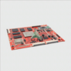
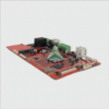
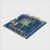
Color Palette: Solder mask pcb colors don’t just serve aesthetics. Black masks help in heat radiation while white and red masks aid in LED applications and prototype identification respectively.
Beyond Gloss: Matte finishes are quickly becoming more popular due to their ability to reduce ambient reflection and enable clearer camera readings during assembly.
UV-Curable Solder Masks: UV-curable masks have become an indispensable resource in PCB manufacturing, helping shorten production cycles while improving environmental friendliness. UV-curable masks could transform this sector.
Solder masks, while often overlooked during PCB manufacturing, play an essential role in its successful functioning and longevity. A full understanding of solder masks – their types, application processes and technological developments – is important for those involved with designing PCBs, manufacturing them themselves or simply seeking innovative electronic solutions. Through this article I aim to shed some light on their significance while encouraging everyone involved with electronic design to stay abreast of emerging trends and remain open-minded towards innovation.
Solder Mask PCB FAQ:
- What is a Solder Mask?
A solder mask is a protective layer applied to the bare printed circuit board (PCB). This layer is designed to prevent solder bridges from forming between closely spaced solder pads during the soldering process. - What are the benefits of using a Solder Mask PCB?
Using a solder mask can increase the reliability of the PCB by preventing short circuits. It also protects the copper traces from oxidation, wear, and environmental damage, aiding in the durability of the PCB. - What materials are used for Solder Mask PCB?
The most commonly used material for solder mask is epoxy liquid photoimageable solder mask (LPSM), due to its ease of application and clarity for imaging processes. - How is a Solder Mask applied to a PCB?
The solder mask is typically applied in a liquid state to the PCB. Once applied, the board is exposed to a powerful light source through a photo-mask. This hardens the mask in the exposed areas, the unhardened mask is then washed away, leaving the protective solder mask on the PCB. - What are the different colors of Solder Mask PCB?
While green is the most common color for solder mask due to tradition and its superior optical properties, solder masks can come in various other colors like blue, red, black, white, and yellow. The color does not generally affect the function of the solder mask. - What is the importance of the Solder Mask PCB opening?
The solder mask opening (or the lack of solder mask) is where the components are to be soldered. Proper sizing of these openings is key to ensuring good solder joints and preventing solder bridging on fine pitch components. - How is the design of Solder Mask done?
The design of the solder mask is usually generated from the PCB design files. The places where components will be soldered are kept free of mask. - What is a Solder Mask Dam?
A solder mask dam refers to the thin wall of solder mask that separates exposed copper pads. It plays a crucial role in preventing the flow of solder from one pad to another, which can lead to solder bridging. - What is a Tenting in Solder Mask context?
Tenting refers to covering via holes using solder mask. This can prevent solder from wicking into the vias during assembly, and can also prevent shorts if vias are close to component pads. - Is Solder Mask always necessary in PCBs?
While solder mask is highly recommended for PCBs involving surface-mount technology and complex designs, it may not be necessary for basic, single-layer PCBs or breadboards, where components are hand-soldered.

