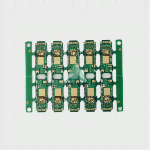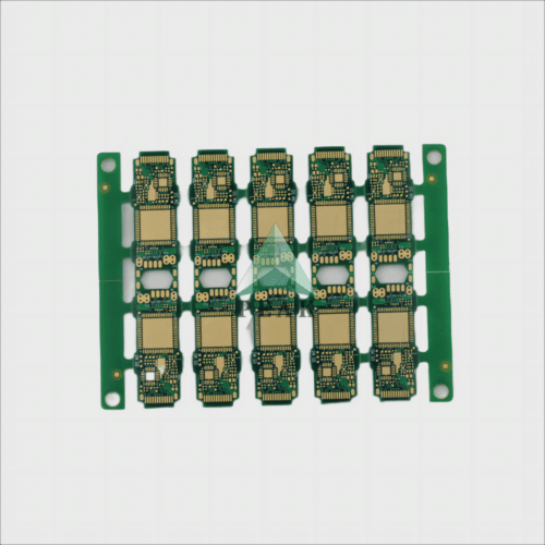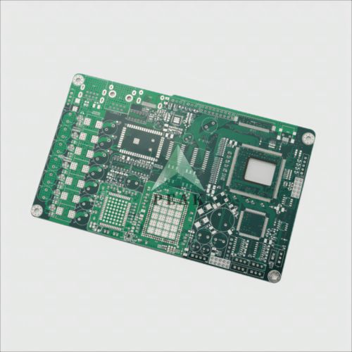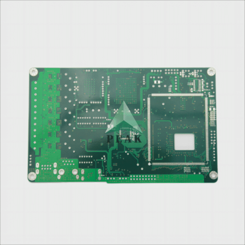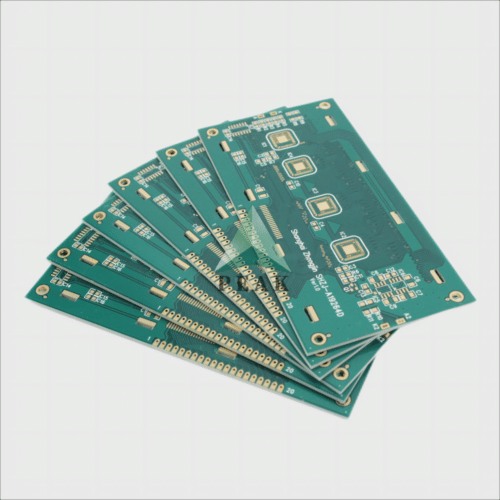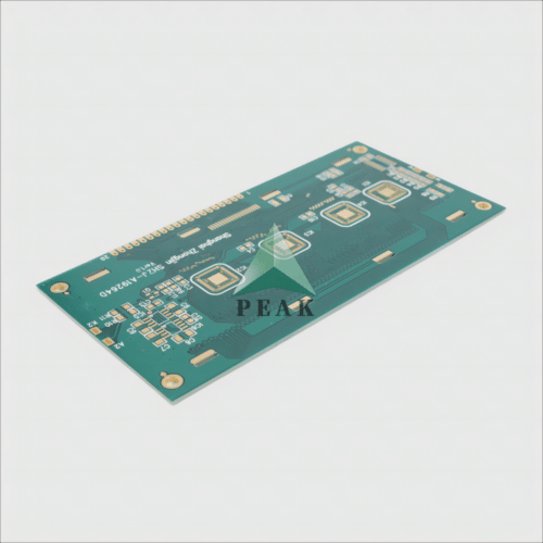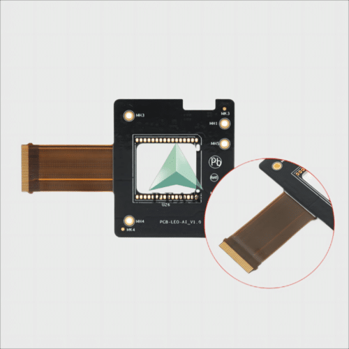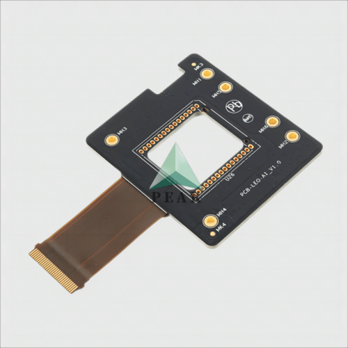
PCB Fabrication
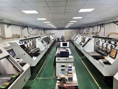
Drilling Machine
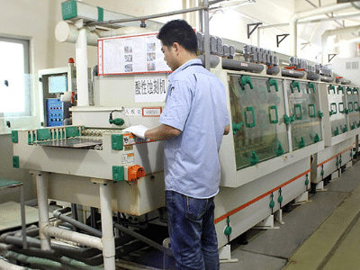
Inner Layer Etching
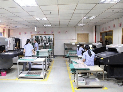
AOI Scanning
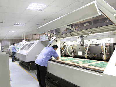
CNC
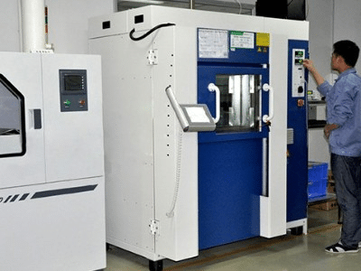
Cold and Heat Shock
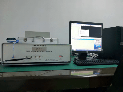
Impedance Tester
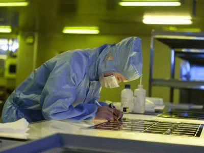
Clean Room
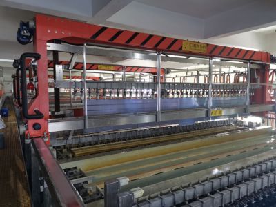
Copper Sinking Line
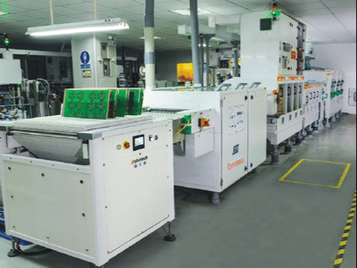
Auto-Development
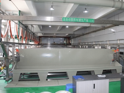
Graphic Plating
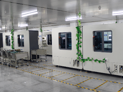
Flying Probe Tester
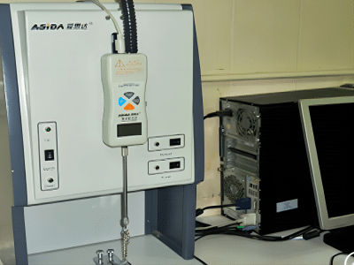
Copper Foil Tensile
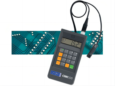
Hole Copper Tester
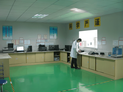
Laboratory
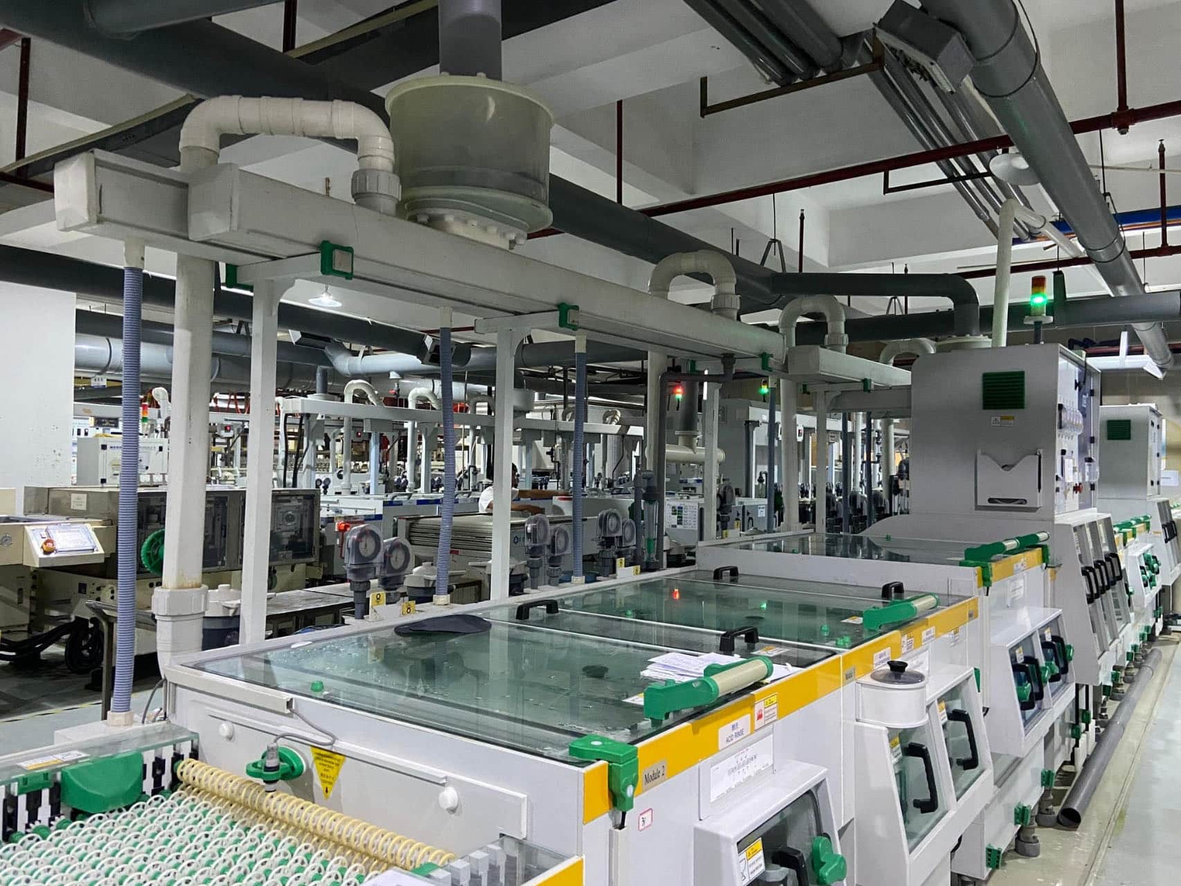
Palm Fiber Line
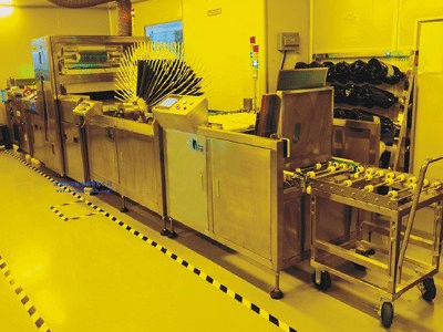
Automatic Laminator
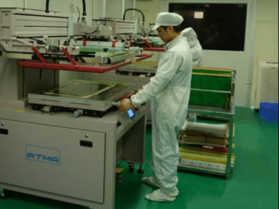
Screen Printing
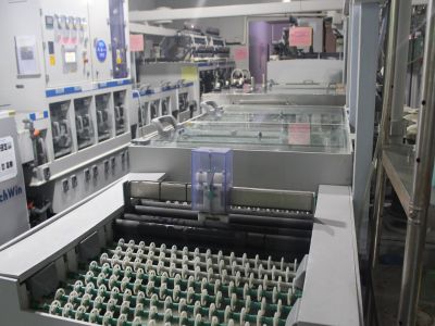
Water Washing
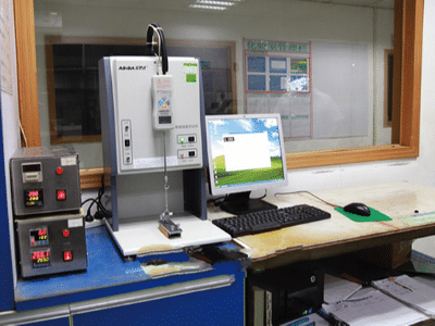
Strong Peel Tester
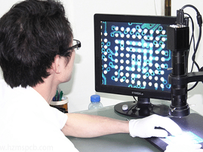
Hundredfold Loupe
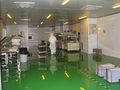
Silkscreen Workshop
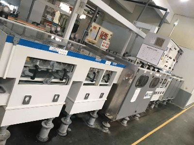
Plate Grinding
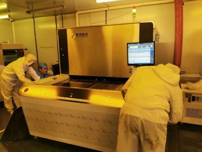
Exposure Machine
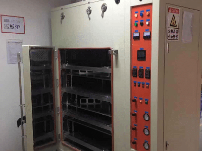
Press Board Furnace
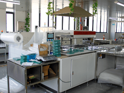
Vacuum Packaging
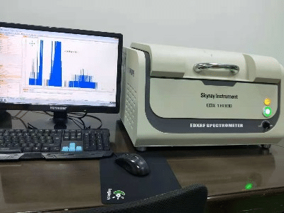
Halogen Tester
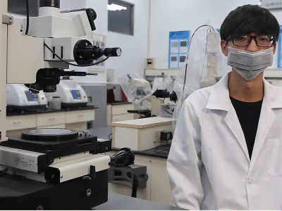
Slicing Analysis
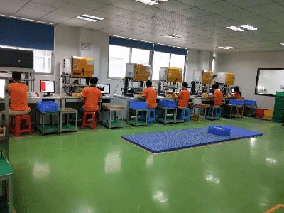
Test Workshop
PCB Assembly
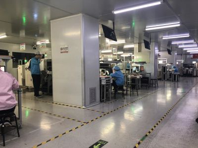
Assembly 1
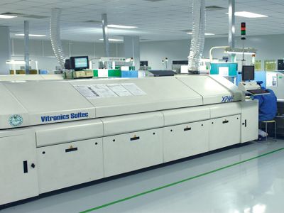
AOI Optical Detector
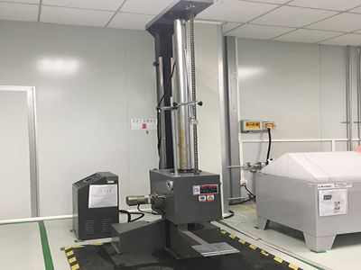
Drop Test
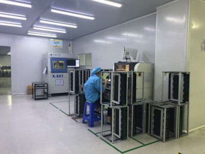
X-Ray
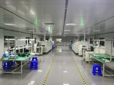
Assembly 2
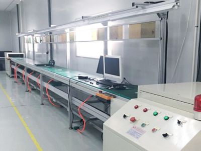
Assembly Welding
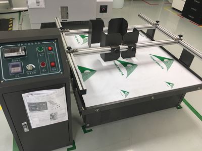
Vibration Testing
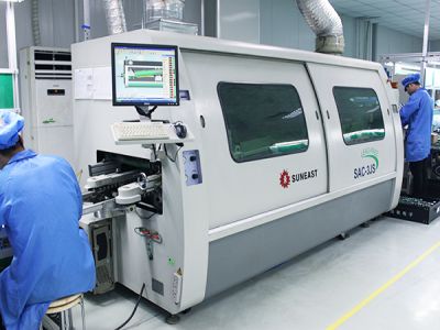
Wave Soldering 1
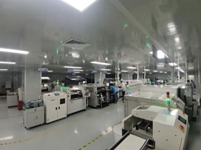
Assembly 3
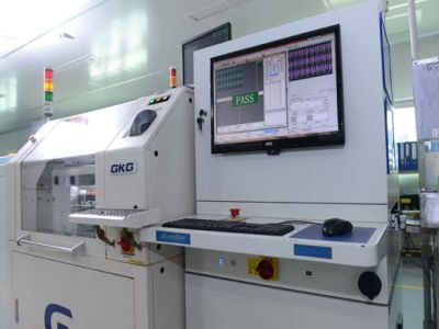
DIP Line
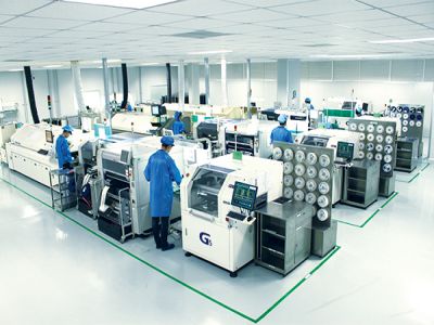
Patch Welding
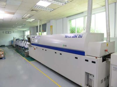
Wave Soldering 2
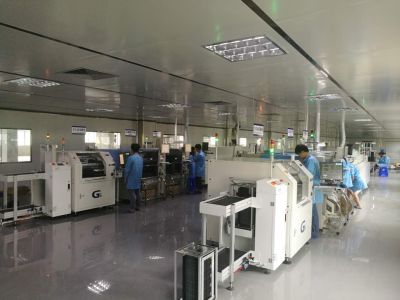
Assembly 4
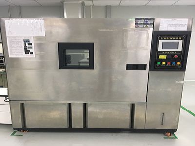
High Temperature Box
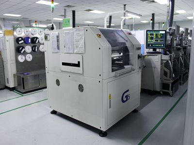
Silk Printer
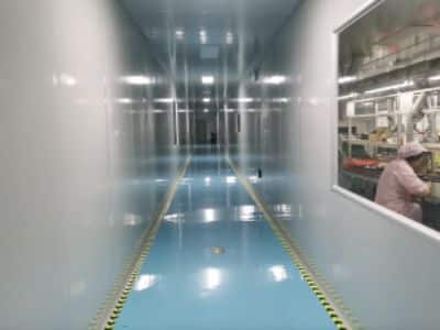
Workshop Corridor
Who is PEAK?
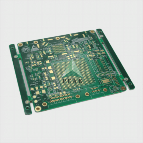
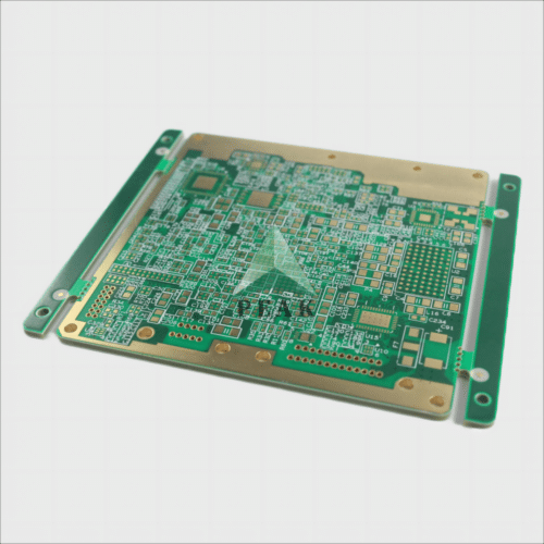
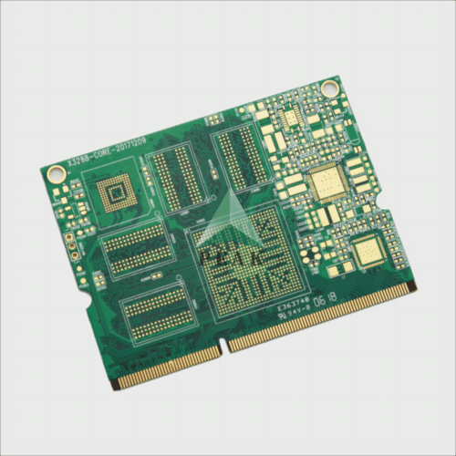
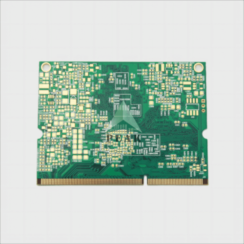
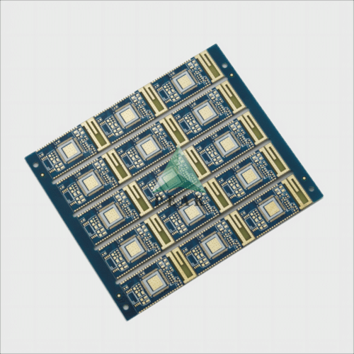
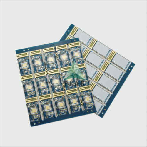
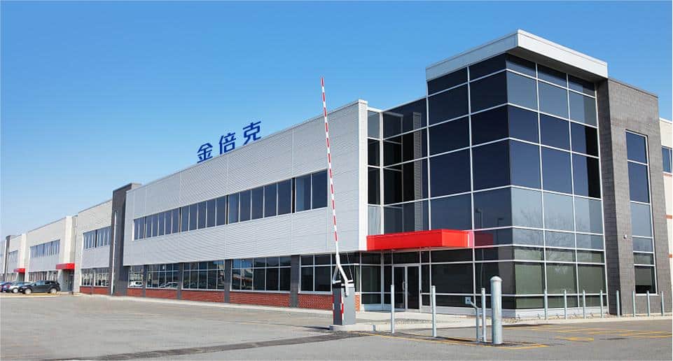
Founded in 2007, PEAK Co.,Ltd is an electronic solutions company offering 1-64 layers PCB fabrication, assembly, testing & validation of rigid, rigid-flex, HDI, high frequency, high speed, metal core, IC substrate, substrate-like and other special PCB. Our modern 54,000 square foot manufacturing facility allows us to provide all rigid & rigid-flex services under one roof and offer quick-turn capabilities.PEAK has a professional reputation for developing high-performance solutions for technically advanced OEM’s in a variety of markets including aerospace and defense, medical, computer, communication, server, semiconductor IC, automotives, industrial control, optoelectronics, LED and others.

Ability to Handle Complex Jobs
All Rigid & Rigid-Flex Services Under One Roof
Regular PCB
Up to 64 Layers; FR4 TG135/TG150/TG170; Halogen Free/CTI≥600; Aspect Ratio (Finish Hole) 28:1; Sample Expedited 8 Hours(1-2Layer);
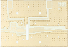
Metal Core PCB
Thermal Conductivity 1-398W/m.K; Aluminum/Copper AC 500-4000V; Post-bonding/Pre-bonding; Sweat-Soldering/Conductive Adhesive; Press-Fit/Embedded Coin(I, T U);
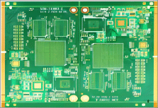
HDI PCB
Blind/Buried/Hybrid Via; 5+N(N+M)+5 Structure; Trace Width/Spacing 1.6/1.6mil; Laser Hole Size(mm)≥0.075; High Density Interconnector;
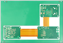
Rigid-Flex PCB
2-24 Layers; Book/Air-gap/Fly-tail; Unsymmetrical/Semi-Flex; Width of Flexible Zone 3mm(min); Dimension Accuracy ±0.05mm(min);
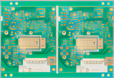
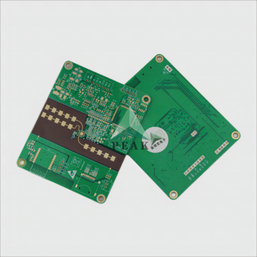
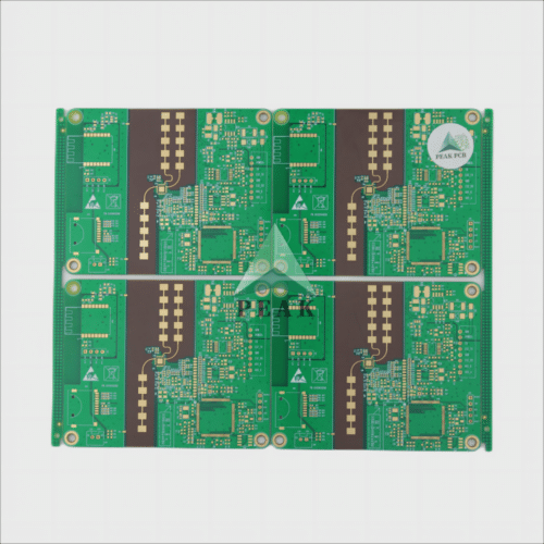
High Frequency PCB
More than 85+ Types; Rogers/Arlon/Taconic/Isola/ Nelco/F4B Serices,etc; Materials can be Specified; Impedance Tolerance ±5%(min);
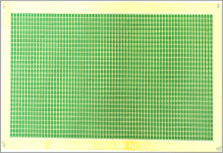
Substrate PCB
CSP/FC-CSP/SIP/FC-BGA/WB-CSP; FR4/BT/High-Speed Material; Trace Width/Space 12/12μm; SM Registration:±20μm; Strict SM Flatness Control ≤5μm;
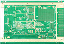
High Speed PCB
Panasonic Megtron4/6/7; TU-872SLK/Isola-FR408HR,etc; Impedance Tolerance ±5%(min); Dimension Accuracy ±0.02mm(min); Line Width/Space Accuracy ±5%;
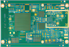
Specialty PCB
Ceramic/Glass Material; Hybrid Material Lamination; Buried Capacitance/Resistance; PTH/NPTH Step Slots; Uneven/Segmented/Step Gold Finger;
Don't Miss Them
The Complete Guide to Etching PCB – A Step-by-Step Process for DIY Enthusiasts
The Complete Guide to Etching PCB – A Step-by-Step Process for DIY Enthusiasts PCB etching is an indispensable skill for creating custom printed circuit boards (PCBs) at home, giving DIY enthusiasts the power to design and fabricate PCBs without outsourcing fabrication services. In this guide, we’ll walk through each step of
The Ultimate Guide to Cleaning PCBs – Tips and Techniques for Effective Maintenance
The Ultimate Guide to Cleaning PCBs – Tips and Techniques for Effective Maintenance Printed circuit boards (PCBs) form the backbone of modern electronic devices. As they contain complex circuits, components, and solder connections that require regular cleaning and maintenance for optimal performance and reliability, PCBs need regular attention as part
Understanding Vias PCB Design: Importance, Types, and Implementation
Understanding Vias PCB Design: Importance, Types, and Implementation Vias are essential components of printed circuit board design, acting as conduits that connect electrical connections between layers of the printed circuit board. Vias serve an important function by maintaining signal integrity, power distribution and thermal management – something we will explore
Understanding PCB Stackup: Importance, Considerations, and Best Practices
Understanding PCB Stackup: Importance, Considerations, and Best Practices PCB stackup refers to the arrangement of layers on a printed circuit board (PCB), including conductors, dielectric layers and any necessary components. It plays an integral part in determining its electrical and mechanical performance; we will explore its importance here as well
Exploring the Global (Printed Circuit Board) PCB Market: Trends, Growth, and Opportunities The printed circuit board (PCB) market plays an integral part of global electronics manufacturing. PCBs are intricately crafted boards used to connect and support electronic components. In this article, we’ll take an in-depth look at this global PCB
A Guide to PCB Repair: Tips and Techniques for Fixing Printed Circuit Boards
A Guide to PCB Repair: Tips and Techniques for Fixing Printed Circuit Boards Printed circuit boards (PCBs) are key components of electronic devices, providing connections for components to communicate and function efficiently. Unfortunately, PCBs may sometimes encounter issues that necessitate repairs; we will provide an extensive guide to PCB repair
Exploring OrCAD PCB Design Software for Efficient Circuit Board Development
Exploring OrCAD PCB Design Software for Efficient Circuit Board Development OrCAD PCB is an innovative design software used extensively in the electronics industry for efficient circuit board development. Thanks to its advanced features and user-friendly interface, OrCAD PCB enables designers to efficiently design complex layouts while validating designs and optimizing
DigiKey PCB Services – Streamlining Your PCB Prototype and Assembly Process
DigiKey PCB Services – Streamlining Your PCB Prototype and Assembly Process Digi-Key Electronics is a globally trusted distributor of electronic components and provides an array of products and services tailored to the needs of engineers, designers, hobbyists, hobbyists and more. One such offering by Digi-Key is PCB services which provide
Mastering the Art of Soldering PCBs – Tips for Successful Assembly Soldering is an integral step in the assembly of printed circuit boards (PCBs), as it creates electrical connections essential for electronic component functioning. Mastering soldering is key for creating reliable connections; in this article we’ll cover techniques and best

