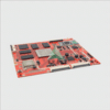
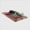
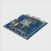
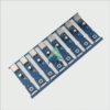
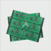
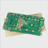
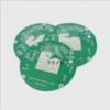
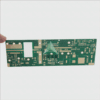
Multilayer thick copper PCB are a specialized type used in circuit board manufacturing. This type of PCB has thick copper layers and is typically used in applications that require high currents and/or high voltages. Because of its ability to carry large amounts of current, it is used in a variety of different industries, including power, electronics, communications, and automotive manufacturing.
When manufacturing multilayer thick copper PCB, thicker copper foil is often used as the base material for the board. This copper foil is typically much thicker than that found on conventional thin copper circuit boards and therefore has a higher current carrying capacity. In addition, multilayer thick copper PCB typically have more layers, which allows them to manage signals and power more efficiently, while also providing better control of heat generation.
In addition to their current carrying capacity, multilayer thick copper PCB have other advantages. For example, they can provide better signal quality and more stable performance. In addition, because they have more layers, the boards are better protected from mechanical damage and environmental factors.
Multilayer thick copper PCB are a very useful type of circuit board with a wide range of applications. If you need to manufacture multi-layer thick copper PCB, it is recommended to consult a professional circuit board manufacturer for more information.
Multi-layer thick copper PCB is a type of printed circuit board (PCB) that is mainly used in high-reliability, high-density and high-performance application scenarios. Its industry standards cover a number of areas, which are described in more detail below.
First of all, the number of layers and thickness of multilayer thick copper PCB is one of its important industry standards. Generally speaking, the number of layers of multilayer thick copper PCB is above 4 layers and the total thickness is above 3mm. These parameters are set mainly to meet the application requirements of high reliability, high density and high performance.
Secondly, the material and structure of multilayer thick copper PCB are also important aspects of their industry standards. Typically, multilayer thick copper PCB use FR4 or CEM-1 as the base material, with a copper layer thickness of 1oz or more. In addition, the structure usually adopts a symmetrical design to ensure the stability and reliability of the PCB.
In addition, the surface treatment of multilayer thick copper PCB is also an important aspect of its industry standard. Common surface treatments include hot air leveling, silver immersion, and gold immersion. These treatments can improve the soldering performance and electrical performance of the PCB to ensure its long-term stable operation.
Finally, the manufacturing process of multilayer thick copper PCB is also an important aspect of its industry standard. High-precision drilling, hole metallization, plating and other processes are usually used to ensure the conductivity and mechanical strength of the PCB. In addition, strict quality control is required in the manufacturing process to ensure that the quality of each batch of products is stable and reliable.
In short, the industry standards for multilayer thick copper PCB involve a number of aspects, including the number and thickness of layers, materials and structures, surface treatment and manufacturing processes. The development and implementation of these standards are of great significance to ensure the quality and performance of multilayer thick copper PCB.

