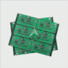
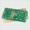
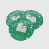
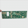
Mastering Double Sided PCBs: A Comprehensive Guide to Understanding and Designing in 2024
As technological innovation rapidly transforms industries, understanding and harnessing double-sided Printed Circuit Boards plays an integral part of leapfrog electronic design. This article offers an all-inclusive guide on double-sided PCBs designed to arm you with all of the knowledge and expertise needed for designing and implementing them successfully in 2024.
Printed Circuit Boards (PCBs) are essential components of many electronic devices, providing essential support by connecting and orchestrating various electronic components. While single-sided PCBs once reigned supreme, double-sided boards have since emerged as an increasingly vital piece of the technological puzzle due to their increased component capacity and compact design.
Understanding Double Sided PCBs
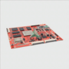
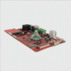
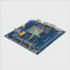
Double-sided PCBs differ from their single-sided counterparts by housing electronic components on both sides. As their name implies, double-sided boards offer many advantages such as increased circuit density, flexible design, faster circuit speeds and enhanced functionality.
Designing Double Sided PCBs: A Step-by-Step Guide
- Comprehending the Basics: Before embarking on your design project, it’s crucial that you comprehend all aspects of a PCB – from its copper substrate to the solder mask that covers it – including their interconnections and protection features.
- Component Placement: Is of critical importance in designing double-sided PCBs. Balancing components evenly on both sides is vital.
- Routing: Once all components have been carefully placed, the next step in the assembly process should be routing. This involves linking them together via copper pathways.
- Soldering: Finally the components should be soldered onto the board to create an integrated circuit of physical and electrical connections between all of their parts.
Double-sided PCB fabrication is the process of manufacturing printed circuit boards with components embedded on both sides. Here is a general overview of the steps involved:
- Design: The first step is to create a design of the circuit board. This is generally done using CAD software. Make sure to verify the design for errors to prevent issues down the line.
- Printing: Once the design is ready, it is then printed using a special printer known as a plotter. This creates what is known as a “film” of the board on a glass epoxy base.
- Copper Prepping: This film is used to prepare a copper plate before it is sent off to the next stage.
- UV Curing: The printed board is then exposed to UV light. This hardens the photo-resist layer and defines the copper paths.
- Etching: The unwanted copper is removed using an etching solution leaving behind the desired copper traces.
- Drilling: After etching, holes are drilled into the board for component mounting.
- Plating and Coating: The board is then electroplated with a thin layer of tin, silver, or gold, and coated with solder mask to protect the circuits.
- Printed and Assembled: Finally, the board is silkscreen printed with the component layout, and components are soldered on both sides.
- Inspection and Testing: The finished PCB goes through rigorous testing to ensure it works as expected.
Remember, this is a general explanation and actual processes may differ based on the service provider or type of printed circuit board being created. It’s always recommended to work with an experienced fabricator that can guide you through each step.
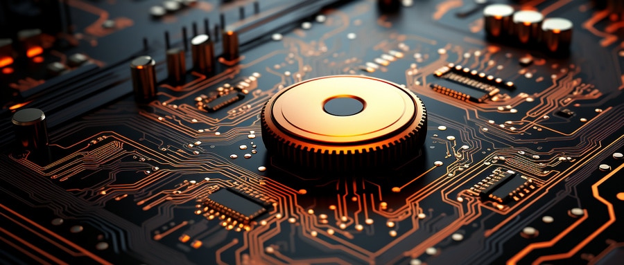
Future Prospect of Double-Sided PCBs in 2024
2024 will see continued demand for advanced electronic devices, necessitating ever more sophisticated double-sided PCBs. New developments are anticipated to further advance their efficiency and capabilities as essential electronic components.
Double-sided PCBs have become an indispensable element of electronics in modern life. By learning their principles and mastering their design process, you can become an essential player in this fast-moving field.
Remember, expertise in double-sided PCBs takes time and dedication to gain. Each bit of knowledge helps bring you one step closer towards becoming a master in this domain; therefore, it is vital that you keep exploring, learning and creating.
This comprehensive guide aims to foster curiosity, spur innovation, and broaden your understanding of double-sided PCBs in line with trends seen today.
FAQ:
- What is a double sided PCB?
A double-sided PCB is a type of printed circuit board that has conductive layers on both of its sides. - What are the uses of double sided PCBs?
Double-sided PCBs are widely used in various technologies and industries including telecommunications, automotive, industrial controls, and power supplies. - How is a double sided PCB made?
Double-sided PCBs are manufactured using a process that starts with a substrate of insulating material, followed by the application of a thin layer of conductive material on both sides. The design is then transferred onto each side. - What is the difference between single sided and double sided PCBs?
A single sided PCB has only one conductive layer, while a double-sided PCB has two. This makes double sided PCBs more complex and able to handle more complicated circuits. - Do double sided PCBs require through-hole technology?
Yes, to enable connections between the layers, double sided PCBs typically require through-hole technology or surface mount technology. - What are the advantages of double sided PCBs?
Double-sided PCBs offer more flexibility in design, increased circuit density, and have a relatively lower cost compared to multi-layer PCBs. - Are double sided PCBs suitable for high-frequency circuits?
While double sided PCBs can be used for a variety of tasks, they may not always be suitable for very high-frequency circuits due to potential interference between the layers of the board. - Is it hard to repair double sided PCBs?
Repairing a double sided PCB can be more challenging than a single sided PCB due to the complexity of the connections, especially if damage occurs in the internal layers of the board. - What materials are used to make double sided PCBs?
The materials used to make double-sided PCBs can vary, but they generally include a substrate material like FR4 and a conductive material such as copper. - Can I design a double sided PCB at home?
Yes, it’s possible to design a double sided PCB at home using various software tools. However, fabricating a double-sided PCB at home can be quite challenging without the right equipment.

