Copper PCBs: A Detailed Exploration into their Functionality and Implementation
PCBs (Printed Circuit Boards) are one of the key components that connect electronic components in most devices. Copper is one of the key materials used in fabricating these boards due to its superior conductivity and versatility; in this article we’ll look at its advantages, applications and manufacturing process as a whole.
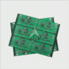
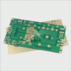
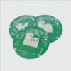
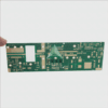
Copper PCBs are electronic boards where all tracks and layers are comprised of copper. Copper offers several advantages that electronics enthusiasts appreciate. One key benefit is Superior Conductivity: copper’s superior conductivity allows devices to perform better electrically.
Copper PCBs are well known for their outstanding Heat Dissipation properties, providing optimal operating temperatures in high performance devices and thus increasing lifespan of devices that incorporate it. Copper’s superior heat conductivity enables it to dissipate heat effectively, helping maintain optimal operating temperatures and prolong device lifespan.
Copper PCBs are also highly reliable. When compared with materials such as aluminum, copper’s superior durability makes it perfect for devices used in challenging environments or require longer lifespan.
Manufacturing a copper PCB involves multiple key steps. First, an electronic circuit design must be approved; once transferred onto copper-clad laminate as the base material for production. Unwanted copper is removed using chemical means until only desired circuit patterns remain; thereafter a layer of solder mask protects these circuits while silkscreen provides component identification before finally soldering completes assembly of the board.
Copper PCBs are widely utilized across a range of electronic devices due to their excellent conductivity and heat dissipation properties, from consumer electronics such as televisions and mobile phones, through more complex systems such as medical equipment, automotive technology and aerospace technology.

Copper PCBs have long been considered an indispensable element in electronic device production. Their excellent conductivity, heat dissipation capacity and durability have made them the go-to material for PCB assembly across industries. An understanding of their fundamental properties will allow designers and manufacturers to make more informed decisions during design and assembly processes that lead to higher performing, more reliable devices.
Join this journey of discovery into the working, applications and advantages of copper PCBs. This comprehensive guide aims to shed light on this essential component of electronics while helping designers, manufacturers and enthusiasts make use of copper PCBs to achieve maximum performance and results.
Copper PCB FAQ:
- What is a Copper Printed Circuit Board?
A copper Printed Circuit Board is a type of printed circuit board (PCB) that utilizes copper as a conductive material in its structure. On these boards, thin copper foil is laminated to an insulating board to form the board’s conductive pathways or “traces.” - What are the Advantages of Copper Printed Circuit Boards?
Copper Printed Circuit Boards offer several advantages, including high thermal conductivity, excellent electrical conductivity, great solderability, and durability. These qualities make them suitable for a wide range of applications, especially where high-performance is a requirement. - How are Copper Printed Circuit Boards Made?
Copper Printed Circuit Boards are made through a complex process that involves applying a layer of copper over a substrate material, and then using a combination of etching and chemical processes to create the required circuitry pattern. - What does OZ Mean in relation to Copper Printed Circuit Boards?
“OZ” stands for ounce per square foot, a unit of measurement that indicates the thickness of the copper layer on the PCB. For example, a 1oz copper PCB means that a one-ounce layer of copper is spread evenly over an area of one square foot on the PCB surface. - How does Copper Thickness affect a PCB’s Performance?
A greater copper thickness enables the PCB to handle higher currents, provides improved thermal management, and improves the mechanical strength of the board. However, this should be balanced with considerations of board weight, cost, and the nature of the electronic application. - What is the Standard Copper Thickness in a PCB?
The standard copper thickness for most PCBs is typically around 1 oz. However, in applications that require high-power or high-temperature operation, heavier copper thicknesses (2 oz, 3 oz, or even thicker) may be used. - How can I Specify the Copper Thickness when Ordering a PCB?
Copper thickness is one of the parameters you can specify when ordering a PCB. This will depend on your specific application requirements. It’s crucial to work closely with your PCB manufacturer to determine the appropriate copper thickness for your project. - What are Heavy Copper Printed Circuit Boards?
Heavy copper Printed Circuit Boards are circuit boards with 3 or more ounces of copper in the inner and outer layers. They are often used for applications that require high power or high heat dissipation, such as power converters and automotive systems. - How long do Copper Printed Circuit Boards Last?
The lifespan of a copper Printed Circuit Board can vary dramatically based on the application, operating conditions, and the quality of the manufacturing process. However, copper is known for its durability and resistance to corrosion, meaning copper PCBs generally have a good lifespan. - How do I Clean Copper Printed Circuit Boards?
Copper PCBs should be cleaned with a mild alcohol-based solution and a lint-free cloth to remove any dirt or oxidation without damaging the board. Avoid abrasive cleaning materials as these can scratch the copper surface.

