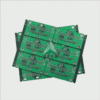
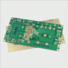
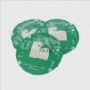
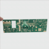
The Power of Multilayer PCBs – Unlocking Advanced Circuit Design
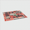
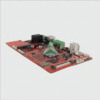
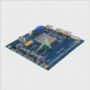
Multilayer PCBs have quickly become an essential element in modern electronics, powering a wide array of devices such as smartphones, computers, and medical equipment. Their ability to accommodate complex circuit designs while providing improved performance have revolutionized printed circuit board technology; in this article we’ll take an in-depth look into this field – exploring its capabilities, advantages, and applications.
What Are Multilayer PCBs?
Multilayer printed circuit boards (PCBs) are multilayered printed circuit boards comprised of multiple conductor traces sandwiched between layers of an insulating material – typically epoxy – usually to provide insulation between each conductor trace layer. Vias establish electrical connections between various layers. While single and double sided PCBs may suffice for basic circuit designs, multilayer PCBs provide the extra space and flexibility required to support more intricate circuitry or high density component arrangements.
Multilayer PCBs present several distinct advantages:
- Compact Design: Multilayer PCBs offer significant space savings compared to single and double sided boards, by stacking multiple layers of conductive traces, components and power/ground planes to reduce size significantly and simplify circuit layout. Their compact designs make multilayer PCBs particularly ideal for applications requiring limited space such as smartphones, tablets and wearable devices.
- Improved Signal Integrity: Electronic devices require strong signal integrity for proper operation, and multilayer PCBs offer improved signal integrity through dedicated power and ground planes that act as shields, minimizing noise interference and electromagnetic interference (EMI), to provide clean and reliable transmission of signals. Separate power and ground planes also aid heat dissipation while decreasing risks associated with thermal issues.
- High-Density Component Integration: Multilayer PCBs excel at accommodating high-density components such as integrated circuits (ICs), microcontrollers and other surface-mounted devices with ease. Their multiple layers offer ample room for routing traces and managing interconnections between components allowing complex circuitry to be implemented within smaller form factors while still providing advanced functionality.
- Noise Reduction: Multilayer PCBs offer excellent noise reduction and electromagnetic compatibility (EMC). By isolating sensitive analog or digital circuitry from power and high-speed signal traces, interference and crosstalk are minimized while ground planes act as shields to lessen external electromagnetic radiation impacting on circuitry.
Manufacturing and Design Considerations:
Multilayer PCB manufacturing processes involve precise layer alignments and lamination techniques to ensure reliable electrical connections. When designing multilayer PCBs, careful consideration must be given to factors like layer stackup, impedance control, signal integrity, thermal management and proper via placement. Working with experienced PCB manufacturers as well as advanced design tools is paramount to successful production and optimal performance.
Applications of Multilayer PCBs:
Multilayer PCBs have many applications within numerous industries and electronic devices, including:
- Telecommunications: Multilayer PCBs have become an essential component in communication systems, network equipment and routers due to their compact design, high density integration and reliable signal transmission properties. They make excellent solutions for these applications.
- Medical Devices: Medical equipment such as diagnostic and implantable devices require high-performance and reliable circuitry to function at their best. Multilayer PCBs offer space for advanced functionality and signal integrity that enable accurate medical diagnoses and treatments.
- Aerospace and Defense: Aerospace and defense industries require robust circuitry that can operate reliably under extreme environments. Multilayer PCBs’ ability to withstand vibration, thermal stress, and provide superior signal integrity make them essential components in avionics, radar, and military communication systems.
- Consumer Electronics: Multilayer PCBs have become an indispensable component in consumer electronics devices like smartphones, tablets, gaming consoles and smart home devices. Their compact designs and efficient functionality facilitate production of sleek yet feature-packed devices.
Multilayer PCBs have revolutionized electronic circuitry, offering compact designs, enhanced signal integrity, and dense component integration. Their importance cannot be understated as they enable the development of smaller yet more powerful devices across many industries. When properly managed during manufacturing processes and design decisions with experienced PCB manufacturers, their applications become endless; take advantage of multilayer PCB’s capabilities for unlocking advanced circuit designs and driving innovation within electronics!
FAQ:
- What is a Multilayer Printed Circuit Board?
A multilayer Printed Circuit Board is a printed circuit board that is composed of more than two copper layers placed between laminate. The number of layers can range from 3 to 14 or more, depending on the complexity of the design. - What are the advantages of Multilayer Printed Circuit Boards?
Multilayer Printed Circuit Boards offer several advantages, including higher assembly density, higher capacity in a smaller space, better noise reduction, increased design flexibility, and improved reliability. - How are Multilayer Printed Circuit Boards produced?
Multilayer Printed Circuit Boards are produced by stacking layers of material, typically copper and insulating materials, in a precise configuration. These layers are then bonded together under heat and pressure to create the final product. - Where are Multilayer Printed Circuit Boards typically used?
Multilayer Printed Circuit Boards are typically used in complex electronic devices that require advanced performance, such as computers, satellite systems, GPS technology, medical equipment, and military communication equipment. - What factors contribute to the cost of Multilayer Printed Circuit Boards?
Key factors include the number of layers, the type and quantity of materials used, the complexity of the design, and the level of customization required. - How can I order Multilayer Printed Circuit Boards?
Multilayer Printed Circuit Boards can be ordered by providing your design files to a PCB manufacturer either directly through their website or via email. - Can Multilayer Printed Circuit Boards be repaired?
Although certain types of damage can be repaired, the process is complex and often requires professional expertise. It’s typically more cost-effective to replace damaged multilayer Printed Circuit Boards. - What is via-in-pad in Multilayer Printed Circuit Boards?
Via-in-pad is a PCB design technique where the via is placed directly in the copper pad. This design enables denser PCBs and allows for smaller trace widths. - What software can I use to design Multilayer Printed Circuit Boards?
Programs like Altium, Eagle, and KiCad are popular software options for designing multilayer Printed Circuit Boards. - How are Multilayer Printed Circuit Boards tested?
Testing procedures for multilayer Printed Circuit Boards typically include visual inspections, electrical tests, and performance tests under different operating conditions.

