Who is PEAK?
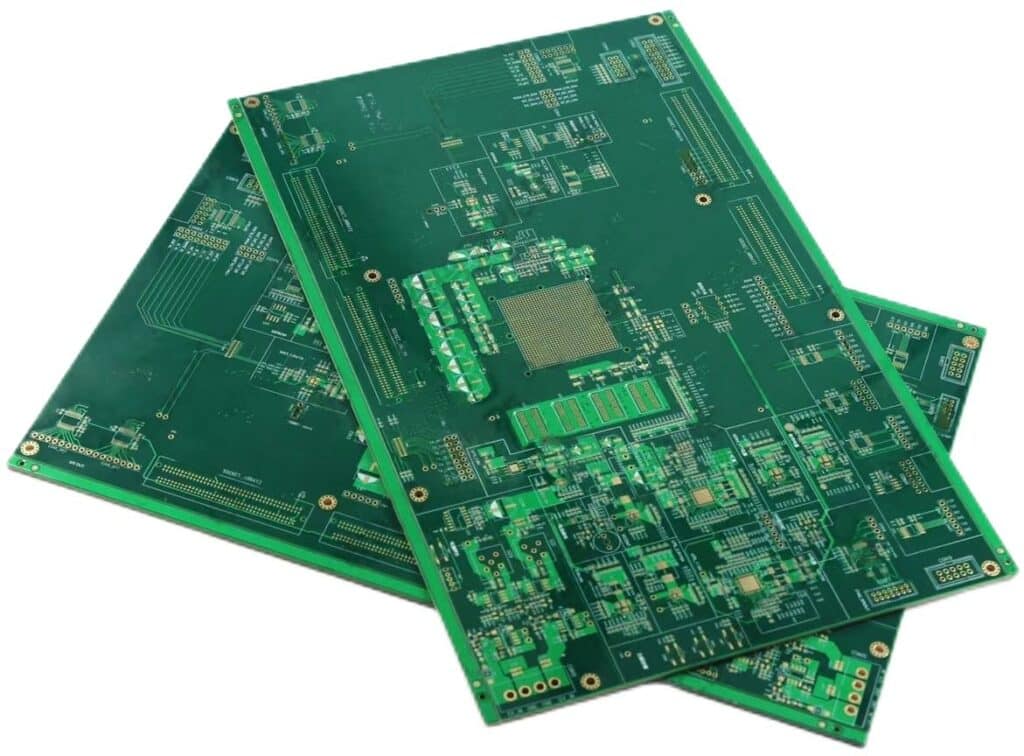
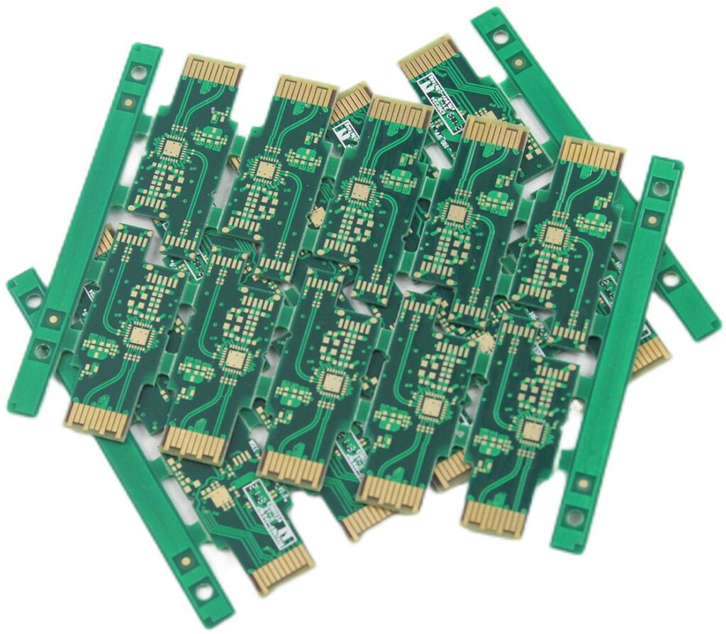
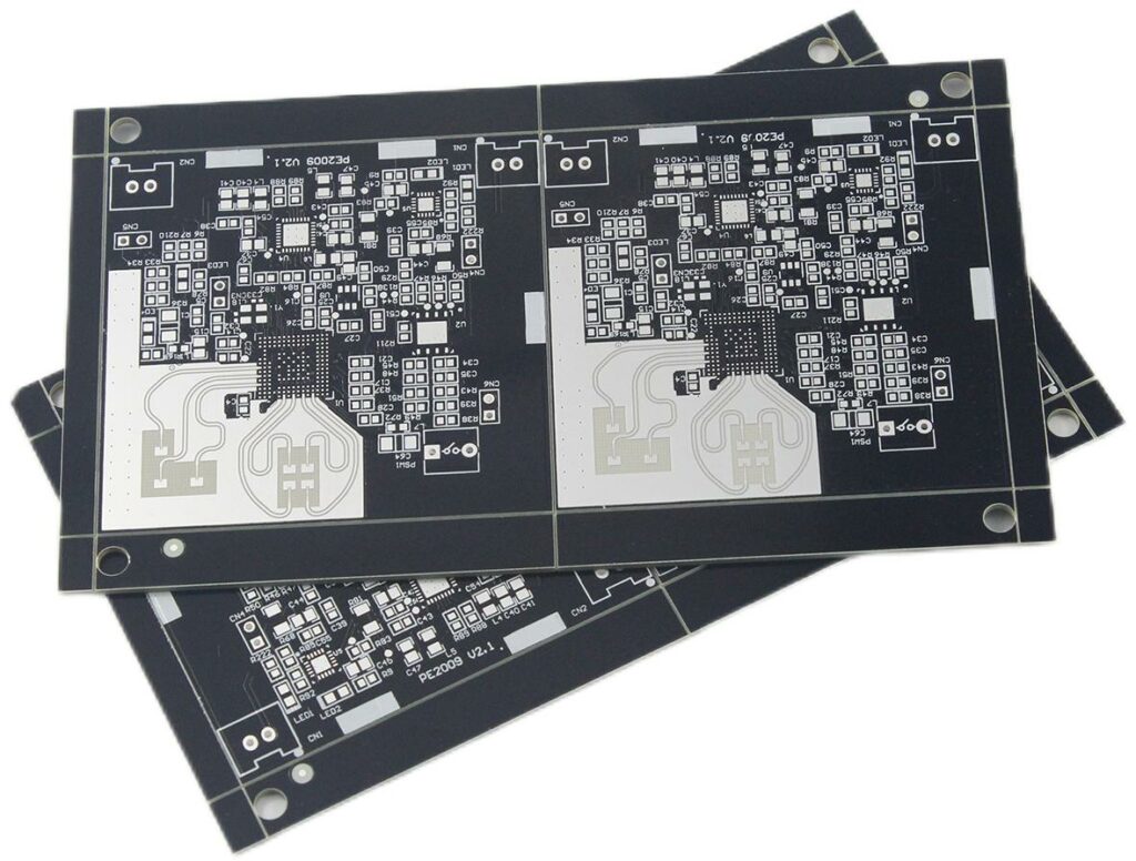
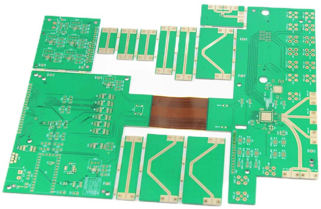
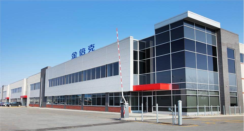
Founded in 2007, PEAK Co.,Ltd is an electronic solutions company offering 1-64 layers PCB fabrication, assembly, testing & validation of rigid, rigid-flex, HDI, high frequency, high speed, metal core, IC substrate, substrate-like and other special PCB. Our modern 54,000 square foot manufacturing facility allows us to provide all rigid & rigid-flex services under one roof and offer quick-turn capabilities.PEAK has a professional reputation for developing high-performance solutions for technically advanced OEM’s in a variety of markets including aerospace and defense, medical, computer, communication, server, semiconductor IC, automotives, industrial control, optoelectronics, LED and others.

Organizational Structure
16 Years Of PCB Manufacturing
1.Founded PEAK Technology in Shenzhen
2.Single Side and Double Side PCB
Fabrication
3.Circuit Board Asssembly Service
4.Samples and Small to Medium Batches
5.Electronic Components Procurement
20 April 2007
PEAK Technology(Shenzhen) Established
1.Founded PEAK Technology in HongKong
2.Started Mass Production(Single Side/Double Side PCB)
3.Start Sample Production(Multilayer PCB)
4.Passed ISO9001/UL/ IATF Certification
5.Overseas Marketing Division Continues to Expand
07 july 2011
PEAK Technology (Hongkong) Established
1.Founded PEAK Electronic in Shenzhen
2.The Production Line was Relocated to Building D, Zhongxi Industrial Park, Bao'an District, Shenzhen
3.Plant Area 11500 Square Meters
4.Total Investment of More than 7.5 Million Dollars
5.Passed ISO14001 Certification
03 July 2013
PEAK Electronic (Shenzhen) Established
1.Xinbao Industrial Park Building A was Added as the Second Production Base
2.Plant Area was Expanded to 54,000 Square Meters
3.Introduced ERP System
4.Passed ISO13485/OHSAS18001 Certification
5.Obtained 8 patents
15 November 2019
Continued Expansion of Production Capacity
1.Passed GJB9001C Certification(China Military Certification)
2.Specialized Processes are Already Available for Mass Production(Resin Plug Hole/Half-Hole/Thick Copper/Gold Finger/Blue Rubber,etc)
3.Accumulated 11 Patents
4.Small Batch Trial Production of IC Substrate&Substrate-Like PCB Samples
08 February 2021
Passed Military Certification
1.Founded PEAK Technology in Dongguan
2.Single Sided Through 64 Layers of PCB Fabrication and Assembly
3.Cumulative Exports to 190+ Countries
4.Over 18,500 Businesses and Innovators Use PEAK PCB
28 October 2023
PEAK Technology (Dongguan) Established
Ability to Handle Complex Jobs
All Rigid & Rigid-Flex Services Under One Roof
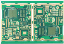
Regular PCB
Up to 64 Layers; FR4 TG135/TG150/TG170; Halogen Free/CTI≥600; Aspect Ratio (Finish Hole) 28:1; Sample Expedited 8 Hours(1-2Layer);
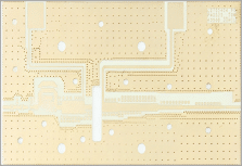
Metal Core PCB
Thermal Conductivity 1-398W/m.K; Aluminum/Copper AC 500-4000V; Post-bonding/Pre-bonding; Sweat-Soldering/Conductive Adhesive; Press-Fit/Embedded Coin(I, T U);
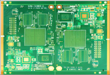
HDI PCB
Blind/Buried/Hybrid Via; 5+N(N+M)+5 Structure; Trace Width/Spacing 1.6/1.6mil; Laser Hole Size(mm)≥0.075; High Density Interconnector;
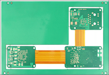
Rigid-Flex PCB
2-24 Layers; Book/Air-gap/Fly-tail; Unsymmetrical/Semi-Flex; Width of Flexible Zone 3mm(min); Dimension Accuracy ±0.05mm(min);
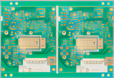
High Frequency PCB
More than 85+ Types; Rogers/Arlon/Taconic/Isola/ Nelco/F4B Serices,etc; Materials can be Specified; Impedance Tolerance ±5%(min);
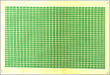
Substrate PCB
CSP/FC-CSP/SIP/FC-BGA/WB-CSP; FR4/BT/High-Speed Material; Trace Width/Space 12/12μm; SM Registration:±20μm; Strict SM Flatness Control ≤5μm;
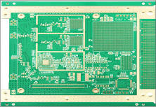
High Speed PCB
Panasonic Megtron4/6/7; TU-872SLK/Isola-FR408HR,etc; Impedance Tolerance ±5%(min); Dimension Accuracy ±0.02mm(min); Line Width/Space Accuracy ±5%;
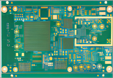
Specialty PCB
Ceramic/Glass Material; Hybrid Material Lamination; Buried Capacitance/Resistance; PTH/NPTH Step Slots; Uneven/Segmented/Step Gold Finger;
Focus On Each PCB Artwork
Fully Certified Defense Capabilities
We have earned a wide variety of certifications that allow us to work with more industry
Areas of Application
Total control of build time and product quality
The Complete Guide to Etching PCB – A Step-by-Step Process for DIY Enthusiasts PCB etching is an indispensable skill for creating custom printed circuit boards (PCBs) at home, giving DIY enthusiasts the power to design and fabricate PCBs without outsourcing fabrication services. In this guide, we’ll walk through each step of PCB etching from creating the […]
The Ultimate Guide to Cleaning PCBs – Tips and Techniques for Effective Maintenance Printed circuit boards (PCBs) form the backbone of modern electronic devices. As they contain complex circuits, components, and solder connections that require regular cleaning and maintenance for optimal performance and reliability, PCBs need regular attention as part of preventive care to stay […]
Contact PEAK
Need pricing fast? Click here and we will get back to you within 4 hours!


