A Comprehensive Guide to HDI PCB (High-Density Interconnect Printed Circuit Board)
HDI PCB (High-Density Interconnect Printed Circuit Board) is an increasingly popular type of printed circuit board due to its numerous benefits for modern electronics design. As demand for smaller and more powerful electronic devices increases, HDI PCB has become more appealing due to its small size, high density interconnections, and enhanced electrical performance. We will examine its various aspects – benefits, applications, manufacturing process – here.
HDI PCB technology brings several distinct advantages that make it the optimal solution for many electronic devices:
- Compact Size: High Density Interconnection PCBs (HDI PCBs) are specifically engineered with compact interconnections and miniaturized components to produce smaller and lighter electronic devices, which makes them especially valuable in industries such as mobile phones, tablets, wearable devices and automotive electronics where space is at a premium.
- Increased Circuit Density: HDI Printed Circuit Boards enable the integration of more components and connections within a smaller area, thanks to microvia technology advancements that allow these boards to accommodate a higher layer count with finer traces for increased circuit density and improved signal integrity.
- Improved Electrical Performance: HDI Printed Circuit Boards offer enhanced electrical performance due to reduced parasitic capacitance and inductance. Their shorter interconnects and optimized trace routing minimize signal losses for faster data transfer rates, lower power consumption consumption, and greater signal integrity.
- Increased Signal Integrity: HDI Printed Circuit Boards’ shorter interconnects and optimized signal routing help minimize electromagnetic interference (EMI) and reflections, improving signal integrity for high-speed applications such as telecom, networking and high performance computing. This feature is essential in high speed environments like telecom, networking and high performance computing environments.
- Design Flexibility: HDI Printed Circuit Boards offer more intricate and complex circuit designs due to their increased layer count and smaller feature sizes, giving designers freedom to add advanced features like blind/buried vias, microvias and fine pitch components for innovative electronic systems.
Application of HDI PCB
HDI PCBs find use in industries and electronic devices requiring high performance and miniaturization. Common applications of these boards are:
- Consumer Electronics: HDI Printed Circuit Boards are widely utilized in consumer electronic devices like smartphones, tablets, smartwatches, digital cameras and gaming consoles, providing both compact size and improved functionality of these devices.
- Automotive Electronics: HDI Printed Circuit Boards have become indispensable components in automotive applications such as advanced driver assistance systems (ADAS), infotainment systems, GPS navigation, vehicle control units and other electronic components. Their compact size and outstanding electrical performance are crucial elements.
- Medical Devices: HDI Printed Circuit Boards offer medical devices a compact and high-density design ideal for implantable devices, diagnostic equipment, and wearable health trackers. Their small form factor makes HDI boards suitable for medical applications.
- Aerospace and Defense: HDI Printed Circuit Boards have found widespread application in aerospace and defense applications where reliability, miniaturization and performance are of key importance – radar systems, avionics, communication systems, military grade equipment and satellites all use HDI Printed Circuit Boards extensively.
- Industrial Automation: Industrial automation systems often demand compact yet high-performance electronics. HDI Printed Circuit Boards can be found in robotics, motor control systems, factory automation and industrial IoT applications to achieve efficient and reliable operation within limited spaces.
Manufacturing Process of HDI PCB
HDI PCB manufacturing process entails several steps, which are described below:
- Design: HDI Printed Circuit Board design incorporates advanced considerations such as high layer counts, fine pitch components, blind and buried vias and microvias to ensure manufacturability. Design software with comprehensive Design Rule Checks (DRCs) are employed for this process.
- Substrate Preparation: PCB substrates are made by laminating multiple layers of copper foil-clad laminate materials together. Depending on their design requirements, these layers may include copper foil-clad laminate materials with dielectric and adhesive features as well.
- Laser Drilling: Laser drilling is an integral component of HDI PCB manufacturing, as it facilitates the formation of small microvias and blind vias with high precision lasers. Holes in substrate material will later be filled in order to form electrical connections.
- Electroplating: After laser drilling, exposed via holes are coated with electrically conductive materials such as copper to establish electrical connections among all layers of a PCB board.
- Copper Deposition and Etching: After deposing copper on the substrate surface, it is then etched away, revealing intricate interconnections. This process must be repeated with every layer to create intricate interconnections.
- Solder Mask Application: Solder masks are applied to protect copper traces and pads while acting as an insulating layer, leaving only openings for vias or pads that need electrical contact to pass through.
- Surface Finish: PCB surfaces must be finished with an anti-oxidation and solderability-enhancing coating to prevent oxidation and ensure solderability, such as Hot Air Solder Leveling (HASL), Electroless Nickel Immersion Gold (ENIG), or Organic Solderability Preservatives (OSP).
- Testing and Inspection: Each HDI PCB that leaves our factory undergoes intensive testing and inspection to verify functionality, electrical connectivity and quality. Various techniques like automated optical inspection (AOI) and electrical testing may be employed during this process.
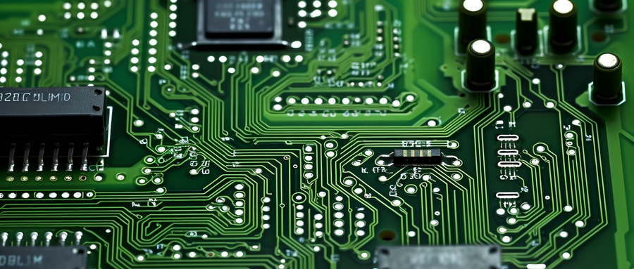
HDI PCBs are an indispensable component of modern electronics industry, enabling compact yet high-performance electronic devices. Their benefits include compact size, increased circuit density, enhanced electrical performance, signal integrity enhancements and design flexibility; HDI PCBs find applications in consumer electronics, automotive electronics, medical devices aerospace & defense and industrial automation applications. Understanding their manufacturing process provides insight into its complex engineering.
FAQ:
- What is an HDI PCB?
HDI stands for High Density Interconnect. An HDI PCB is a circuit board that uses a higher wiring density than traditional PCBs, typically featuring finer lines, smaller vias, and higher layer counts. - What are the benefits of using HDI PCBs?
HDI PCBs can offer several benefits including improved electrical performance, reduced weight and size, enhanced design efficiency, and increased circuit density. - What are Microvias?
Microvias are small (often less than 150 microns in diameter) holes in a PCB used to connect different layers of the PCB. They’re typically used in HDI PCBs to save space and improve electrical performance. - Are HDI PCBs more expensive than traditional PCBs?
Generally speaking, due to the increased complexity and finer features required, HDI PCBs can be more expensive to produce than traditional PCBs. - Which industries typically use HDI PCBs?
HDI PCBs are commonly used in industries where size, weight, and advanced functionality are important, like smartphones, tablets, medical devices, aerospace and automotive electronics, and more. - How is an HDI PCB designed?
Similar to standard PCBs but with extra considerations for routing density, microvias, and multilayer stack-up. The process usually involves advanced CAD software. - What are the typical layer counts for HDI PCBs?
HDI PCBs can have many layers, typically ranging from 4 to 16 or more depending on the complexity of the design. - What are blind and buried vias?
Blind vias connect the outer layer to inner layers without going through the entire board. Buried vias connect internal layers and are not visible from the outer layers. Both are often used in HDI PCBs to save space. - What challenges are associated with manufacturing HDI PCBs?
The small features and high layer counts of HDI PCBs can present challenges in drilling, etching, stacking, and testing, requiring advanced production methods and careful quality control. - How can I verify the quality of an HDI PCB?
You can look at a manufacturer’s certifications (like ISO 9001), use of quality materials, testing processes, and customer reviews. Quality HDI PCBs should have precise features with no defect and stable performance.

