Decoding PCB Panel Sizes: A Detailed Guide to Optimization & Efficiency
At this stage in electronics and technology development, Printed Circuit Boards (PCBs) cannot be understated in their significance. PCBs serve as the control center, connecting various components together so devices may function seamlessly. Before we delve into its functionality however, we must first understand its structure – starting with its unique panel sizes. Let us embark on this adventure to unpack and comprehend this world of PCB panel sizes!
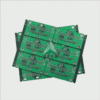
Once we understand what exactly a PCB panel is, let’s move onto its definition – PCB panel sizes. Assuming you already have some understanding about what a PCB panel entails, here is our simple definition: A PCB panel is defined as an interconnect circuit board consisting of multiple smaller boards known as PCBs that are then disassembled individually into individual units. Now that we understand what exactly a panel entails let’s move onto how big one should be!
PCB panel sizes are determined by individual PCB dimensions, the configuration of boards on a panel and assembly process requirements. Standard panel sizes for PCBs are 18 x 24 inches and 21 inches. Custom sizes may also exist to enclose individual PCBs.
Recognizing the principles behind panel size definition is central to achieving efficiency and cost-effectiveness in PCB manufacturing. An optimal panel size helps minimize waste while optimizing material utilization – contributing significantly towards cutting manufacturing costs and decreasing waste levels.
An additional key consideration when choosing PCB panel sizes is ease of fabrication and assembly. Panel dimensions must allow for safe handling during manufacturing while fitting easily into machines used for assembly.
Quality-wise, having a well-defined panel size helps limit potential board warping during fabrication, leading to improved output quality and higher rates of assembly success in thermal cycles.
As technology develops, PCB panel sizes change accordingly. Handling smaller PCB sizes may require specific tooling or assistance during assembly – which is where panel optimization comes in to play – to minimize waste while optimizing efficiency, which is essential to meeting modern PCB production demands.
Finally, let us not overlook the significance of panel break-off areas, commonly known as breakout tabs or scores, which allow for easy separation of individual boards from a panel. Their width must be factored into PCB panel sizes.
Conclusion PCB panel sizes can be complex, demanding careful calculation and optimal usage to maximize efficiency, cost-effectiveness and quality. Accurate PCB panel sizes play a pivotal role in successful PCB manufacturing; their accuracy reveals much about its overall performance.
Our guide seeks to bridge the gap between PCB panel sizes and your understanding, helping you appreciate all of their finer details of electronics manufacturing. An ideal PCB panel size may only represent part of an intricate manufacturing journey; nonetheless it sets an important precedent.
So the next time you look at an electronic device, don’t overlook its simple yet essential panel size – something often forgotten by consumers and manufacturers alike. PCB manufacturing requires getting this right as well – remember it all starts with panel size!
PCB Panel Size FAQ:
- What is a PCB Panel?
A PCB panel is a larger board that consists of multiple smaller boards (or PCBs). The smaller boards are arranged in the panel and are separated after the assembly process. - Why are PCBs Panelized?
PCBs are panelized to streamline the manufacturing and assembly process. By grouping several smaller boards on a larger panel, manufacturers can assemble more boards at the same time, increasing efficiency and lowering costs. - What are the standard PCB Panel Sizes?
The panel size depends on the manufacturer’s capabilities and the client’s requirements. However, common sizes usually range from 18 by 24 inches or 16 by 22 inches. - How is the Size of the PCB Panel determined?
The size of the panel is determined by factors such as the size of the individual PCBs, the capabilities of the manufacturing and assembly equipment, and the cost implications of various panel sizes. - What is the space needed between PCBs on a Panel?
The space between individual PCBs on a panel is typically 2 to 3mm to allow space for the depaneling cut. - What is Depaneling?
Depaneling is the process of separating the individual PCBs from the panel once the assembly process is completed. This can be done by methods such as routing, laser cutting, or manual breaking, depending on the panelization method used. - Can I have different designs on the same Panel?
Yes. This concept is known as a Multi-Project Panel (MPP) or Panel Sharing, which accommodates different PCB designs on the same panel. - How are PCBs held together in a Panel?
Techniques to keep PCBs together on a panel can include V-grooving, where a ‘V’ channel is cut into the top and bottom of the panel between the PCBs, or perforated (tab-routed) holes which can be broken to separate the boards. - How to choose the right Panel Size?
The ideal panel size often involves a balance between maximizing the number of PCBs on the panel, minimizing waste, and maintaining compatibility with manufacturing and assembly equipment capacities. - Do all manufacturers have the same Panel Size?
No, the panel size can vary between different manufacturers. It’s generally best to consult with your manufacturer to determine optimal panel dimensions based on their capabilities and your project’s demands.

