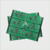
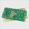
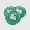
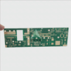
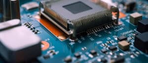
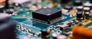
Comprehensive Guide to PCB Inspection: Ensuring Quality & Reliability
Due to unprecedented advancements in technology and electronics, demand for high-quality Printed Circuit Boards (PCBs) has skyrocketed. Understanding its role in quality assurance is integral for electronics manufacturing industry; thus this article is dedicated to PCB inspection processes; specifically the various methods and tools utilized by industry to guarantee quality and reliability – taking you through every aspect of this essential process.
PCB inspection refers to the practice of inspecting PCBs during their manufacturing stages in order to detect flaws or deviations from design that might compromise functionality in finished products. Its importance cannot be overstated: defects could lead to device failure that compromise not only quality and reliability of product but also manufacturer reputation if left undetected; inspection is thus essential in maintaining consistency, quality, and reliability in electronic production.
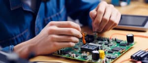
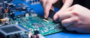
PCB inspection methods vary significantly, each with their own set of advantages and disadvantages. Manual inspection is the starting point, providing skilled workers with a first line check of any visible defects on PCBs. While manual inspection requires skill and intensity from skilled workers, human capabilities remain an limiting factor that often limits results.
Automated Optical Inspection (AOI), one of the most widely-used PCB inspection techniques, has become increasingly popular due to automation’s superior results. Utilizing high-definition cameras and intelligent software, AOI identifies defects such as shorts, opens, missing components or incorrect ones quickly and reliably.
Automated X-ray inspection (AXI), another advanced automated inspection method, offers an invaluable glimpse of PCB layers to detect hidden faults that AOI cannot, such as inadequate solder bridges or voids.
Recently, we have seen dramatic advances in PCB inspection technologies. AI (Artificial Intelligence) combined with Machine Learning algorithms is ushering in an age of automated inspection – where not only defects are detected but they are predicted and avoided as well.
PCB inspection’s future looks bright, with smart manufacturing concepts like IoT (Internet of Things), big data and advanced robotics offering sustainable quality and reliability in PCB production. Thanks to such breakthroughs, inspection is expected to become more accurate and efficient while drastically increasing production quality while simultaneously decreasing operational costs.
Manufacturing firms can utilize PCB inspection to ensure only top-grade PCBs reach customers, and any issues are quickly identified and rectified before final assembly begins. This attention to detail helps maintain an outstanding reputation for quality and reliability while simultaneously cutting wasteful costs.
Conclusion PCB inspection is an integral step to quality assurance in PCB manufacturing, and with advances in technology the future looks bright for automated inspection methods that combine artificial intelligence (AI) capabilities and machine learning algorithms with various techniques aimed at revolutionizing its approach, making it more cost-effective, reliable and time efficient than ever.
Our comprehensive guide aims to offer valuable insight into the world of PCB inspection, giving you insight into its essential role in maintaining electronic product quality and reliability. Whether you work within manufacturing or as an interested consumer, understanding PCB inspection is vitally important in today’s tech-driven society.
Remember, every PCB we encounter begins as an unshielded copper sheet and, through design, etching, drilling, assembly and testing processes culminates in a functioning PCB. But even after assembly has taken place and testing completed, only through reliable PCB inspection can we be assured these boards fulfill their purpose with efficiency and perfection.
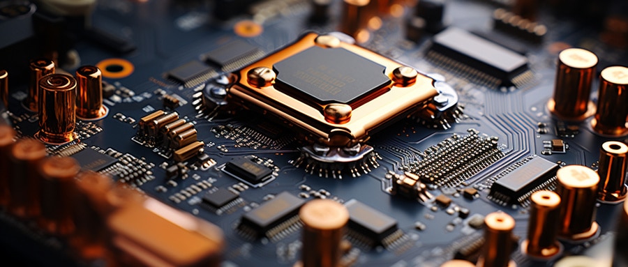
Quality and reliability require adapting to cutting-edge technology, and PCB inspection offers the promise of moving forward together with this world of constant technological change.
At present and for the foreseeable future, excellence in PCB inspection equals quality electronics. That is the formula for success in our increasingly digital world. So the journey continues; each inspection taking us one step closer towards mastering electronic manufacturing as an art and science.
PCB Inspection FAQ:
- What is Printed Circuit Board Inspection?
Printed Circuit Board inspection is a critical part of the PCB manufacturing and assembly process. It involves checking the board at various stages to identify any potential defects or issues that may affect the final functionality. - Why is Printed Circuit Board Inspection necessary?
Printed Circuit Board inspection is crucial to ensure the quality and reliability of the final product. It helps to detect errors or defects early in the process, which can save time and cost in the long-run. - What types of defects could PCB Inspection catch?
Printed Circuit Board Inspection aims to catch any kind of defect that could affect the final product’s operation. This might include soldering defects, incorrect or missing components, shorts or open circuits, incorrectly drilled holes, and other physical or electrical irregularities. - What are the methods of Printed Circuit Board Inspection?
Common methods of Printed Circuit Board inspection include visual inspection, automatic optical inspection (AOI), X-ray inspection, and In-Circuit Testing (ICT). - What is Visual Printed Circuit Board Inspection?
Visual inspection is the most basic type of Printed Circuit Board inspection, usually performed by a quality assurance engineer who examines the board for obvious defects such as missing components or physical damage. However, it’s not as effective for detecting more subtle defects. - What is Automatic Optical Inspection (AOI)?
AOI uses high-definition cameras and special software to capture and compare images of the PCB against the standard design. It can detect issues like missing, incorrect or reversed components, insufficient solder, and short circuits. - What is X-Ray Inspection?
X-ray inspection is used to inspect areas of a PCB that are not visible to the naked eye or an optical system. It’s typically used to check the quality of leadless or BGA (Ball Grid Array) components, through-hole fill, solder joints, etc. - What is In-Circuit Testing (ICT)?
ICT is a type of Printed Circuit Board inspection that checks every installed component for correct value/function and verifies solder joint integrity. It requires a “bed of nails” test fixture that contacts all the test points on the PCB. - What is Functional PCB Testing?
Functional testing is a type of PCB inspection that tests the final assembly under operational conditions. The board is powered and tested to ensure it operates as expected. - What software is used in Printed Circuit Board inspection?
Various types of software are used in PCB inspection, depending on the inspection equipment. Traditional AOI systems use image-processing software, while X-ray systems may use more advanced 3D imaging software. More automated systems will use machine learning or AI-based software for more efficient defect recognition.

