Science of PCB Stencils: A Comprehensive Guide in 2024
At the core of electronics lies Printed Circuit Board (PCB) stencils – templates used for applying solder paste in precise places on bare circuit boards for surface mount assembly – play an indispensable role. While they’re often overlooked, PCB stencils play an integral part in ensuring efficiency and effectiveness for any electronic device; therefore, this article offers an insightful guide into their design, application, evolution, significance in today’s tech-driven society and offers tips for their usage.
At the start of any journey into PCBs, it is vital to gain an understanding of what a PCB stencil entails. Simply stated, this device is a thin board which contains cutout designs of PCB layout. When used during assembly of electronic components, solder paste can easily adhere to this incredible architectural marvel and help apply solder to its surfaces.
Over the years, PCB stencils have played an essential role in meeting the ever-evolving demands of modern electronics. Surface Mount Technology (SMT) introduced laser cut stencils that provide higher precision than their chemically etched predecessors; today’s top-of-the-line stencils are precisely cut according to exacting specifications to ensure precise assembly of intricate designs and smaller components.
PCB stencils play an essential role in SMT manufacturing – one of the cornerstones of modern electronics production. Their accuracy and speed allow mass component assembly onto PCBs for quicker manufacturing processes that ultimately decrease time from concept to product.
PCB stencils cannot be understated as these tools play an integral part in the quality of electronic products. First, they ensure an even application of solder paste across the board; secondly, they enable accurate placement of components that improve reliability and performance of end products. Acknowledging their importance requires thorough consideration by professionals working in electronics industries or similar fields.
Selecting an effective PCB stencil requires careful consideration of many variables. From type (laser-cut or chemically etched), thickness and type of material used, aperture size and size all play an integral part. In addition, solder paste inspection plays a pivotal role as well in making sure only enough solder is being applied during assembly.
Given the constant advances in technology, PCB stencils look set for an exciting future. As techniques, designs, and materials evolve in response to ever more complex electronic devices requiring stencils; ultimately PCB stencils will continue to shape electronics manufacturing, underpinning innovation and driving progress forward.
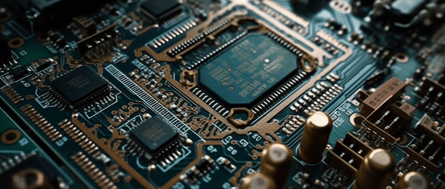
PCB stencils are essential parts of electronic device production, serving to promote efficiency, precision, and overall product quality. As such, their presence warrants further education and awareness on this crucial component. This comprehensive guide seeks to educate readers about PCB stencils while initiating discussions regarding their role in an increasingly tech-dependent world.
PCB Stencil FAQ:
- What is a PCB Stencil?
A Printed Circuit Board (PCB) stencil is a sheet of metal or plastic with holes cut in the exact places and sizes where solder paste is to be applied on the PCB. It enables precise application of the paste which is critical to the high accuracy of Surface Mount Technology (SMT) assembly processes. - What materials are used to make PCB stencils?
The most common material used for PCB stencils is stainless steel due to its durability and stability. However, for low-volume production or prototyping, plastic stencils may also be used because of their lower cost. - How does a PCB Stencil work?
During the assembly process, the stencil is aligned with the PCB, and a spreader or squeegee is used to push the solder paste through the holes in the stencil and onto the PCB. Once the stencil is lifted off, a precise amount of solder paste remains on the PCB at each of the pad locations. - What types of PCB stencils are there?
There are mainly four types: laser-cut stencils, chemical etch stencils, electroformed stencils, and cast stencils. Laser-cut stencils are the most commonly used due to their accuracy and consistency. - How do I decide on the stencil thickness?
The stencil thickness generally depends on the smallest component on your board. As a rule, smaller components such as 0201s and fine pitch QFPs will need thinner stencils, while larger components can accommodate thicker stencils. Your PCB assembly house will likely have guidelines on this. - Can a stencil be reused?
Yes, stencils can typically be cleaned and reused multiple times. However, they will eventually wear out, particularly if they are plastic. - What are Fiducial marks in PCB stencil?
Fiducial marks are reference points on PCB and stencil, which allow the assembly machine to accurately locate and align the stencil over the PCB. They are usually circular with a clear surrounding area. - How can we ensure optimal solder paste release from the stencil?
This depends on factors like the smoothness of the stencil walls, solder paste type, stencil thickness, and the squeegee technique. It’s important to ensure that these factors are properly adjusted during the process to achieve optimal solder paste release. - Can I make my own stencil?
While it’s technically possible to make your own stencil, it usually requires specialized cutting machines for precision, so it’s generally more advisable to have it made by professional manufacturers. - Can I design a stencil using PCB design software?
Yes, most PCB design software have the capability to generate stencil designs along with the PCB layout. The stencil design (also known as the paste layer) can be exported as a Gerber file and then used by the stencil manufacturer.

