PCB Classics: 8 classic PCB problems explained
Engineers must not only prevent PCB boards from being damaged during the production and processing, but they also have to prevent design errors. This article summarises and analyses three common PCB issues, in the hope of being able to help you with your design and manufacturing work.
PCB problems 1: PCB Short Circuit
A: The PCB board is one of the most common failures and can cause this problem in many ways. We will analyze each one.
To prevent short circuits, you can increase the distance between points and pads, or change the round pad to an oval.
The same board will short-circuit if the PCB design direction is incorrect. It is very easy to short circuit if the SOIC feet are parallel to the wave. At this point, you can modify the direction of parts so that they are perpendicular.
It is possible that the automatic insertion will result in a short circuit on the PCB. Because of IPC requirements of the length and angle of the foot, which is 2mm or less, when parts fall, it’s easy to cause a short circuit. You need to leave more than 2mm between the soldering point line.
Engineers can check and compare these reasons with the faults that occur.
PCB problems 2: The PCB board looks dark with granular joints
A: The formation of solder joints is too fragile. Dark color may be caused by low tin solder.
Solder is another reason, the composition changes of the solder during the manufacturing process. Too much impurity in the solder, you need to replace it or add pure tin. Stained glass is caused by the physical changes that occur in the fiber layers, such as the separation of layers. This is not an example of a bad joint. This is because the substrate has become overheated. Reduce the soldering and pre-heating temperatures or increase the substrate’s speed.
PCB problems 3: PCB solder joints turn golden yellow in color
A: Generally, solder on PCB boards is gray. However, there may be golden yellow solder joints. This problem is primarily caused by a high temperature. At this time, lowering the temperature in the tin-furnace can solve the issue.
PCB problems 4: Is the board’s bad affected by the environment?
A: Due to the design of the PCB, if it is placed in an unfavorable atmosphere, the board can be damaged. Conditions such as extreme temperatures, variable temperatures, excessive humidity, vibrations of high intensity and others can lead to a board’s performance being reduced or scrapped. Changes in ambient temperatures, for example, can lead to deformation. Solder joints may be damaged, board shapes bent or copper traces broken.
Moisture in the air, on the other hand can cause corrosion, oxidation and rust to metal surfaces, such as solder joints, pads, component leads, and exposed copper traces. A buildup of dust, dirt or debris on board and component surfaces can reduce airflow, resulting in PCB overheating. Vibrations, drops, hits or bending of the PCB may cause it to deform and crack. High currents and overvoltage could also cause the PCB’s components to age faster.
PCB problems 5: PCB Open Circuit
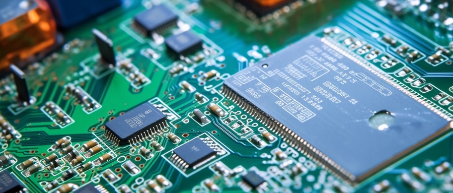
A: An open circuit is when the trace breaks or the solder only covers the pads, not the leads of the component. There is no connection or adhesion between the PCB and the component in this case. These can occur in the same way as short circuits during manufacturing, soldering or other operations. Vibrating, stretching or dropping the boards or any other mechanical deformation factor can damage the solder joints or traces. Solder or metal components can also wear out due to moisture or chemical agents. This leads to component lead breaking.
PCB problems 6: Misaligned or loose components
A: During the reflowing process, some small components can float and detach themselves from the solder joint. Other possible causes of tilting or displacement include vibrations or bouncing components on the PCB, due to insufficient board support, reflow settings, solder paste problems, human error etc.
PCB problems 7: Soldering problems are discussed.
A: Poor soldering can cause a number of problems.
Solder joints that are disturbed: External disturbances cause the solder to move before it has a chance to solidify. It is similar to cold solder joints, but the cause is different. This can be corrected by heating and cooling the joint while there are no outside disturbances.
Cold Soldering occurs when solder is not melted properly, leading to rough surfaces and unreliable connection. Excess solder can also cause cold solder joints. Reheat the joint to remove excess solder.
Solder Bridges are formed when two leads physically connect together by solder crossing. They can form shorts and unexpected connections that could cause components to burn or lose alignment when the current is high.
Solder pads: insufficient wetting of leads or pins. Soldering too much or not enough. Raise pads caused by overheating or rough-soldering.
PCB problems 8: Human error
Human error is the main cause of most defects in PCB production. Up to 64% or more of all avoidable defects are caused by faulty production processes. This includes misplacing components, unprofessional manufacturing techniques, and faulty production methods. As the circuit becomes more complex, the likelihood of defects will increase. This is due to factors such as densely packed components, multiple circuit layers and delicate alignments.
There are many challenges in the design and production processes that lead to PCB board issues.
Poor soldering may lead to problems such as short circuits and open circuits. Cold solder joints are also possible. Misalignment can cause poor contact, resulting in poor performance. Poorly insulated copper traces may lead to arcing.

