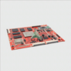
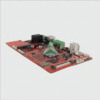
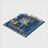
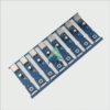
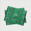
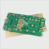
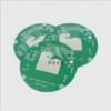
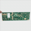
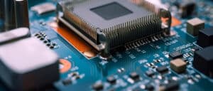
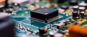
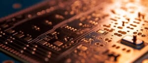
PCB thick gold plate, let the electronic equipment fly higher and farther
PCB thick gold is a kind of thick metallization technology used in the production process of PCB (Printed Circuit Board), which improves the electrical conductivity and mechanical strength of PCB by covering the surface of PCB with a thick metal layer. This technology is mainly used in high-reliability, highly integrated electronic equipment, such as aerospace, military, communications and other fields.
The production process of PCB thick gold is relatively complex and requires multiple steps. First, a metallized layer is coated on the surface of the PCB, usually using processes such as gold immersion or electroplating. Then, the metal layer is thickened by hot pressing or electroplating, etc., so that it reaches the desired thickness. Finally, the PCB is processed and tested to ensure that its electrical conductivity and mechanical strength meet the requirements.
The main advantage of PCB thick gold is that it improves the conductivity and mechanical strength of the PCB while reducing signal interference and transmission delays between circuits. In addition, it also improves the wear and corrosion resistance of the PCB, extending its service life.
However, PCB thick gold also has some disadvantages. First, the manufacturing cost is higher due to the complex production process. Second, due to the thicker metal layer, it may affect the signal transmission quality and timing stability of the PCB. In addition, the manufacturing process requires the use of a large number of chemicals and energy, which has a certain impact on the environment.
PCB thick gold is an important technical means to improve the performance of PCBs, which is suitable for highly reliable and highly integrated electronic devices. Although there are some drawbacks, its application prospect is still very broad under the continuous technical improvement and environmental awareness.
- PCB Thick Gold, or Circuit Board Thick Gold Manufacturing, is an advanced technology in the field of electronics manufacturing. It mainly involves covering a PCB (Printed Circuit Board) with a layer of metal to increase its electrical conductivity and mechanical strength. This technology has demonstrated unique advantages in many applications.
- PCB thick gold can significantly improve the conductivity of the circuit board. Since the conductivity of metal is much better than insulating materials, the thick gold cover makes the circuit board conductivity has been greatly improved. This is essential for high frequency, high power and high speed electronic devices.
- PCB thick gold can enhance the mechanical strength of the circuit board. Metallic materials have good tensile, compressive and impact resistance, so the thick gold cover can effectively enhance the durability of the circuit board, so that it can work stably in harsh environmental conditions.
- In addition, PCB thick gold also has excellent corrosion and oxidation resistance. The metal material can effectively prevent the erosion of oxygen and moisture on the circuit board, thus extending the service life of the circuit board.
- PCB thick gold also has good aesthetic and decorative properties. By choosing different colors of metal materials, the board can achieve high performance, but also has a good appearance and branding.PCB thick gold advantages are mainly reflected in the improvement of electrical conductivity, mechanical strength, corrosion and oxidation resistance, as well as good aesthetics and decorative aspects. These advantages make PCB thick gold in the field of high-end electronics manufacturing has a wide range of application prospects.

