All Rigid & Rigid-Flex Services Under One Roof
PCB Fabrication In As Little As 8 hours
Quotation: [email protected]
Engineering: [email protected]
Ability to Handle Complex Jobs
All Rigid & Rigid-Flex Services Under One Roof
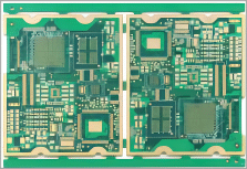
Regular PCB
Up to 64 Layers;
FR4 TG135/TG150/TG170;
Halogen Free/CTI≥600;
Aspect Ratio (Finish Hole) 28:1;
Sample Expedited 8 Hours(1-2Layer);
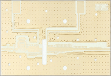
Metal Core PCB
Thermal Conductivity 1-398W/m.K;
Aluminum/Copper AC 500-4000V;
Post-bonding/Pre-bonding;
Sweat-Soldering/Conduct Adhesive;
Press-Fit/Embedded Coin(I, T U);
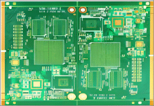
HDI PCB
Blind/Buried/Hybrid Via;
5+N(N+M)+5 Structure;
Trace Width/Spacing 1.6/1.6mil;
Laser Hole Size(mm)≥0.075;
High Density Interconnector;
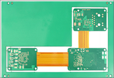
Rigid-Flex PCB
2-24 Layers;
Book/Air-gap/Fly-tail;
Unsymmetrical/Semi-Flex;
Width of Flexible Zone 3mm(min);
Dimension Accuracy ±0.05mm(min);
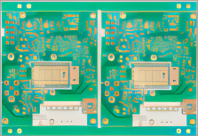
High Frequency PCB
More than 85+ Types;
Rogers/Arlon/Taconic/Isola/
Nelco/F4B Serices,etc;
Materials can be Specified;
Impedance Tolerance ±5%(min);
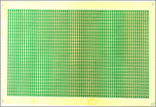
Substrate PCB
CSP/FC-CSP/SIP/FC-BGA/WB-CSP;
FR4/BT/High-Speed Material;
Trace Width/Space 12/12μm;
SM Registration:±20μm;
Strict SM Flatness Control ≤5μm;
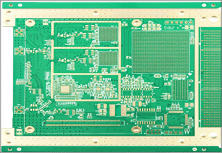
High Speed PCB
Panasonic Megtron4/6/7;
TU-872SLK/Isola-FR408HR,etc;
Impedance Tolerance ±5%(min);
Dimension Accuracy ±0.02mm(min);
Line Width/Space Accuracy ±5%;
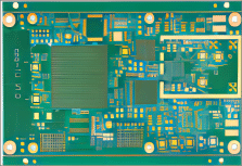
Specialty PCB
Ceramic/Glass Material;
Hybrid Material Lamination;
Buried Capacitance/Resistance;
PTH/NPTH Step Slots;
Uneven/Segmented/Step Gold Finger;
Who is PEAK?
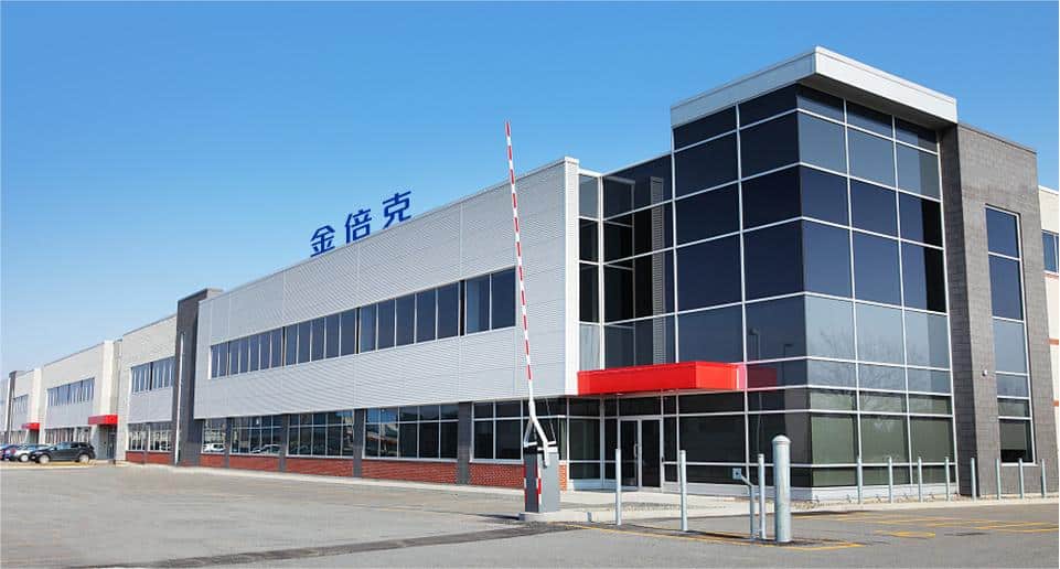
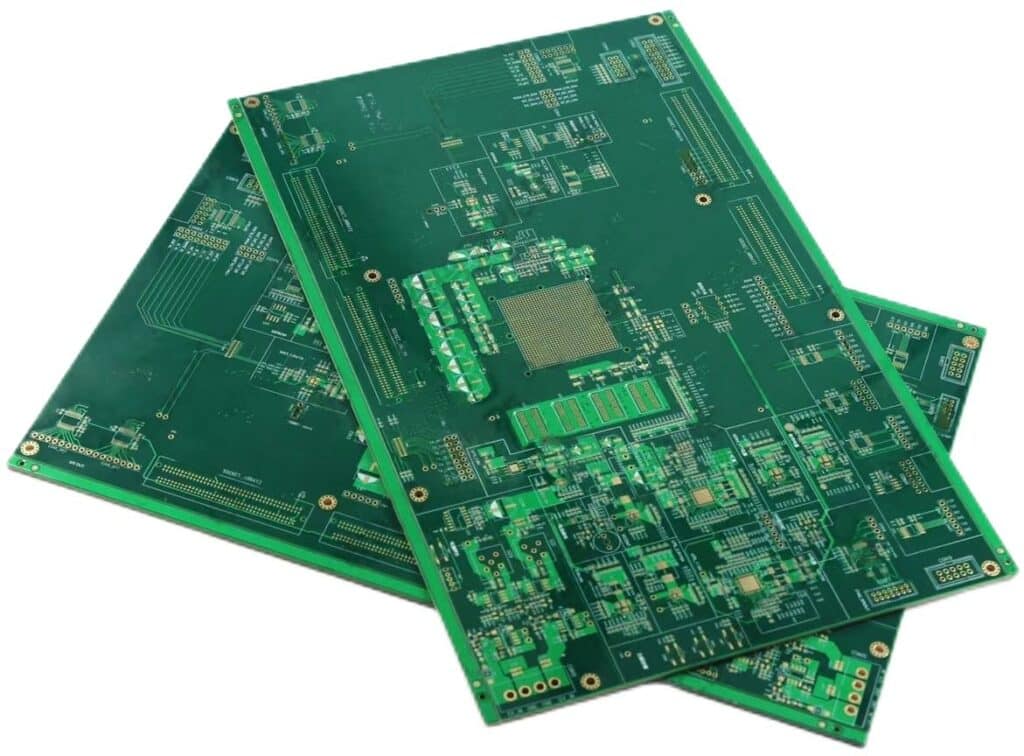
Founded in 2007, PEAK Co.,Ltd is an electronic solutions company offering 1-64 layers PCB fabrication, assembly, testing & validation of rigid, rigid-flex, HDI, high frequency, high speed, metal core, IC substrate, substrate-like and other special PCB. Our modern 54,000 square foot manufacturing facility allows us to provide all rigid & rigid-flex services under one roof and offer quick-turn capabilities. PEAK has a professional reputation for developing high-performance solutions for technically advanced OEM’s in a variety of markets including aerospace and defense, medical, computer, communication, server, semiconductor IC, automotives, industrial control, optoelectronics, LED and others.
Fully Certified Defense Capabilities
We have earned a wide variety of certifications that allow us to work with more industry
Eleven Patents For PCB Production Protection
Military Certified PCB Fabrication & Circuit Board Assembly Manufacturer
Why PEAK PCB?
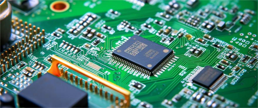
Superior Material
- Well-known FR4 material brands, such as SYTECH,ITEQ,TUC,EMC,KB,etc.
- With over 120+ material types stored in our warehouse, there is no limit to design development.
- The quality of the finished PCB is stable with KuangShun/TAIYO solder mask.
- PEAK has established a conflict minerals policy, management system and investigation framework consistent with the relevant legislation and is committed to not using conflict metals.
Advanced Equipments
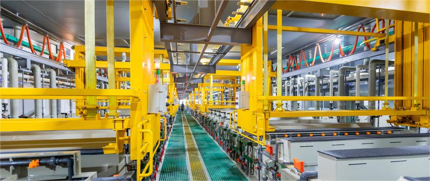
- 16 years of proven laminating technology and equipment allow us to laminate up to 64 layers with ease.
- Advanced exposure machine makes 1.6 mil trace width/spacing achievable.
- Innovative solder mask production lines allow us to control SM flatness to less than 5 microns.
- Fully-automatic PCB test machines significantly reduce product delivery time.
Attentive Service
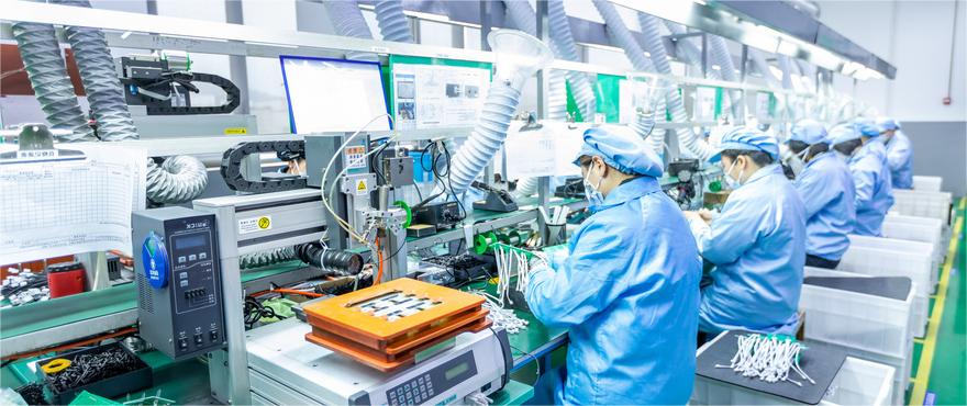
- Custom PCB service and after-sales is service available 24/7.
- Recommend a reasonable project production schedule based on your budget.
- Quotation time is within 6 hours(standard) and will not exceed 48 hours(innovative).
- File review before production to avoid error of production.
Fast Delivery
- The monthly Board capacity of 32,000㎡ gives us more confidence in quick delivery.
- PEAK have 45+ CAM engineers to meet your needs for quick quotes and gerber file processing.
- PCB and assembly lines are all under one roof, which reduces the delivery time of products.
- Stable logistics partners such as DHL/Fedex/UPS/TNT enable faster and on-time delivery of products.

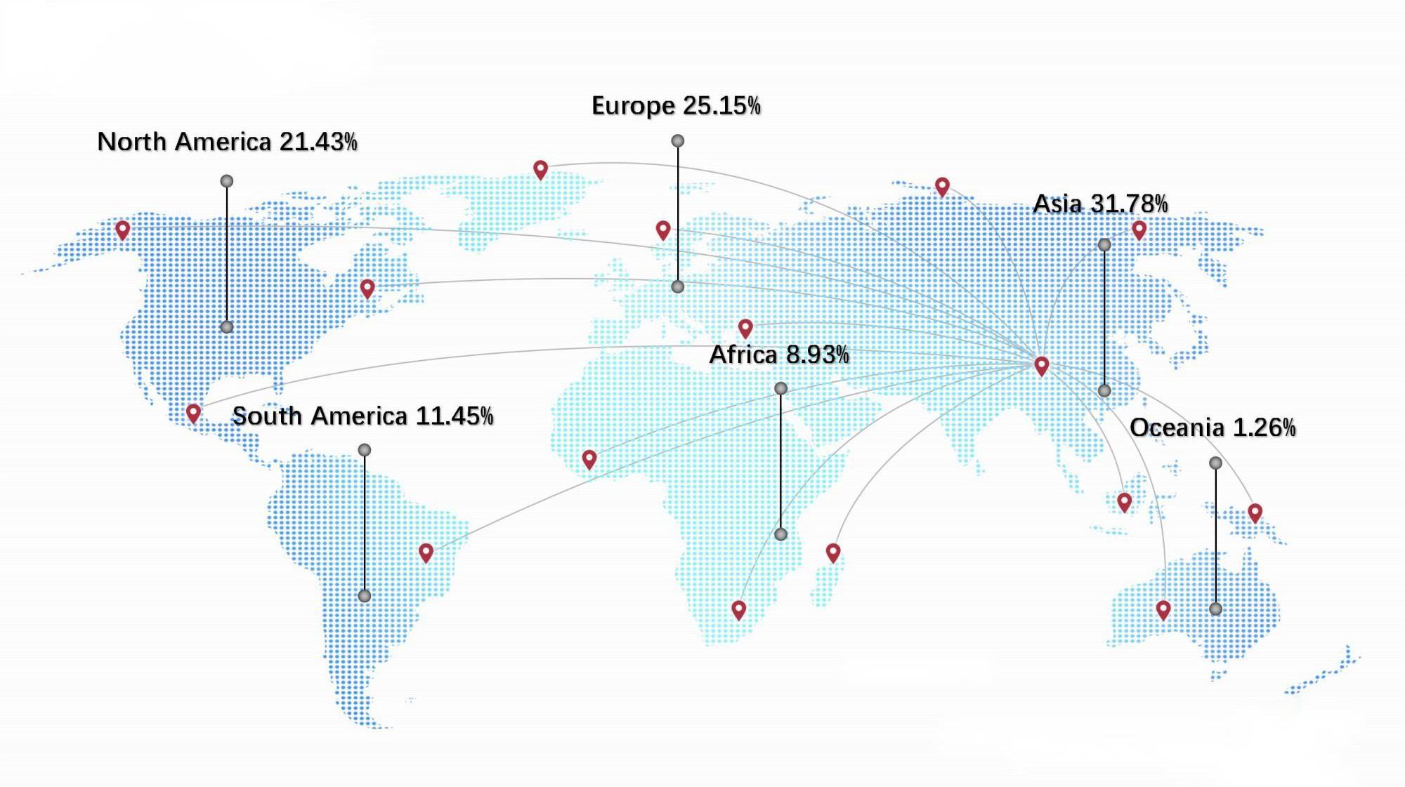
Global Market Distribution
Capacity
Footprint
Fabrication
Engineer
Quotation
On-Time
Countries
Partners
Focus On Each PCB Artwork
Strict Material Selection
All branded materials are used and the raw materials are tested for all indicators and returned immediately if they fail.

Precision machining
LDI laser exposure machine, vacuum etching machine, character inkjet printer and many other imported equipment, processing accuracy greatly improved
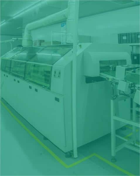
Full product inspection
Each production step has QC special inspection, operator self-inspection, QA sampling product control layer by layer

Functional guarantee
Secondary elements, copper thickness tester, impedance tester gold thickness tester and other imported instruments and equipment to ensure performance

PCB Assembly Service
- One-Stop Fabrication and Assembly
- Flexible Volume Assembly Alternatives
- Comprehensive Quality Assurance
- Parts Sourcing
- High Efficiency, Low Cost
- Professional Engineering Team
- SMD, through-hole and mixed assembly
- 5-7 days lead time including components
- 100% FAl, SP1, AOI checking
- Surface-mounting and through-hole soldering
- 1206,0805,0603 components SMT technology
- ICT,FCT technology
- PCB Assembly With CE,FCC,Rohs Approval
- Nitrogen gas reflow soldering technology
- Siemens siplace D1/D2 & siemens siplace S20/F4
- FolunGwin FL-RX860 & FolunGwin ADS300
- Aleader ALD-H-350B,X-RAY Testing Service
Areas of Application
Total control of build time and product quality
Have Other Questions About PEAK?
Contact now, let us take care of your needs
Q1: What is needed for PCB/PCBA quotation?
For PCBA projects, please provide the same information as above, and include a BOM list and pick and place file.
If you are interested in turnkey services that include programming and functional testing, please contact us for more details. I hope this is what you were looking for. Let me know if there's anything else I can assist you with.
Q3: What’s your minimum of quantity(MOQ) ?
We understand that different businesses have different needs, and we are committed to providing our customers with the best possible service and meeting their specific production requirements.
Q5: What other service do you have?
Q7: What is your testing policy and how you control the quality?
Q2: Are my files safe?
We have strict measures in place to ensure that all documents shared with us are kept confidential and are never shared with third parties.
If needed, we are willing to sign a non-disclosure agreement (NDA) in accordance with local laws to maintain the highest level of confidentiality for your data.
Please feel confident that your information is protected throughout our entire process.
Q4: How to calculate the shipping cost,delivery time?
1-8 layers PCB fabrication---------- 8-72 hours
10-24 layers PCB fabrication----------- 5-10 days
26 layers and above PCB fabricaion---------- Needs assessment



































.jpg)
.jpg)
